
EP3CLS200F484C7N
| Part Description |
Cyclone® III Field Programmable Gate Array (FPGA) IC 210 8211456 198464 484-BGA |
|---|---|
| Quantity | 746 Available (as of June 15, 2026) |

| Product Category | Field Programmable Gate Array (FPGA) |
|---|---|
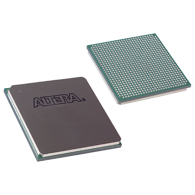
| Manufacturer | Intel |
| Manufacturing Status | Active |
| Manufacturer Standard Lead Time | 26 Weeks |
| Datasheet |
Specifications & Environmental
| Device Package | 484-FBGA (23x23) | Grade | Commercial | Operating Temperature | 0°C – 85°C | ||
|---|---|---|---|---|---|---|---|
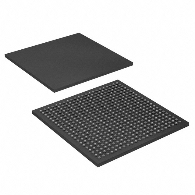
| Package / Case | 484-BGA | Number of I/O | 210 | Voltage | 1.15 V - 1.25 V | ||
| Mounting Method | Surface Mount | RoHS Compliance | RoHS Compliant | REACH Compliance | REACH Unaffected | ||
| Moisture Sensitivity Level | 3 (168 Hours) | Number of LABs/CLBs | 12404 | Number of Logic Elements/Cells | 198464 | ||
| Number of Gates | N/A | ECCN | 3A991D | HTS Code | 8542.39.0001 | ||
| Qualification | N/A | Total RAM Bits | 8211456 |
Overview of EP3CLS200F484C7N – Cyclone® III Field Programmable Gate Array (FPGA) IC, 198,464 logic elements, ~8.21 Mbits RAM, 210 I/Os, 484-BGA
The EP3CLS200F484C7N is an Intel Cyclone® III family FPGA offering high logic density and substantial on-chip memory in a compact 484-ball BGA package. Built on the Cyclone III device architecture, this part targets high-volume, low-power, cost-sensitive commercial applications that require extensive programmable logic, abundant embedded memory and a generous I/O complement.
With 198,464 logic elements and approximately 8.21 Mbits of embedded RAM, the device is suited for designs that need significant logic and data buffering on-chip while operating within a commercial temperature range and a 1.15–1.25 V core supply window.
Key Features
- Logic Capacity Approximately 198,464 logic elements provide a large, flexible fabric for complex combinational and sequential logic implementations.
- Embedded Memory Approximately 8.21 Mbits of on-chip RAM (8,211,456 bits) for frame buffers, FIFOs, lookup tables and soft-state storage without relying on external memory.
- I/O Count 210 user I/Os offering ample external connectivity for high-pin-count interfaces and multi-channel designs.
- Low-Power Family Architecture Cyclone III device family is optimized for low power via TSMC low-power process technology and a power-aware design flow to help meet strict energy budgets.
- Clock Management Family-level clock resources include four phase-locked loops (PLLs) per device with five outputs per PLL for flexible clock synthesis and distribution.
- Supply Voltage Core voltage range specified at 1.15 V to 1.25 V for precise power delivery and compatibility with family power domains.
- Package & Mounting 484-ball FBGA (23 × 23) in a surface-mount BGA format for compact board integration and high I/O density.
- Operating Range & Grade Commercial grade device rated for 0 °C to 85 °C operation.
- Environmental Compliance RoHS compliant.
Typical Applications
- High-volume consumer systems On-chip logic and memory enable feature-rich consumer products where cost and power are constrained.
- Portable and battery-powered devices Low-power family architecture helps extend battery life for handheld products requiring significant programmable logic.
- Communications and networking Large logic capacity and abundant I/Os support packet processing, protocol bridging and multi-channel interface implementations.
- Industrial automation and instrumentation (commercial deployments) Use for sensor aggregation, user-interface control and deterministic logic tasks within commercial-temperature systems.
Unique Advantages
- High-density programmable fabric: 198,464 logic elements deliver the headroom to integrate complex state machines, datapaths and control logic on a single device.
- Significant on-chip memory: Approximately 8.21 Mbits of embedded RAM reduce external memory dependency and simplify board-level BOM and layout.
- Flexible I/O and package: 210 I/Os in a 484-FBGA (23×23) footprint provide a balance of connectivity and compact PCB real estate.
- Family-level low-power design: Built on TSMC low-power process technology and supported by power-aware design flows to help your end product meet power targets.
- Robust clock resources: Multiple PLLs and multi-output clocking options simplify clock domain creation and high-speed interface timing.
- Commercial-temperature reliability: Rated for 0 °C to 85 °C and RoHS compliant for standard commercial deployments.
Why Choose EP3CLS200F484C7N?
The EP3CLS200F484C7N positions itself as a high-capacity, low-power Cyclone III FPGA option for designers needing substantial on-chip logic and memory within a commercial-temperature device and compact BGA package. It combines family-level low-power optimizations and clock-management resources with a large I/O complement to address demanding system-level integration without excessive external components.
Supported by Cyclone III family resources such as clocking primitives and pre-built IP available for the family, this device suits teams building scalable, cost-sensitive commercial products that benefit from a mature FPGA ecosystem and well-defined design flows.
Request a quote or submit a purchase inquiry to receive pricing and availability for EP3CLS200F484C7N. Our team can help evaluate fit for your design and supply immediate ordering information.


Date Founded: 1968
Headquarters: Santa Clara, California, USA
Employees: 130,000+
Revenue: $54.23 Billion
Certifications and Memberships: ISO9001:2015, ISO14001:2015, ISO17025:2017, ISO27001:2022, ISO45001:2018, ISO50001:2018


