
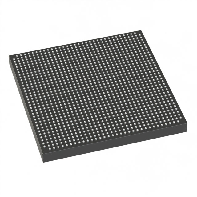
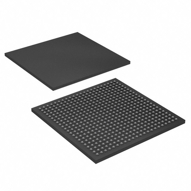
EP3SE110F1152C2N
| Part Description |
Stratix® III E Field Programmable Gate Array (FPGA) IC 744 8936448 107500 1152-BBGA, FCBGA |
|---|---|
| Quantity | 1,093 Available (as of June 12, 2026) |

| Product Category | Field Programmable Gate Array (FPGA) |
|---|---|
| Manufacturer | Intel |
| Manufacturing Status | Obsolete |
| Manufacturer Standard Lead Time | Contact Us |
| Datasheet |
Specifications & Environmental
| Device Package | 1152-FBGA (35x35) | Grade | Commercial | Operating Temperature | 0°C – 85°C | ||
|---|---|---|---|---|---|---|---|
| Package / Case | 1152-BBGA, FCBGA | Number of I/O | 744 | Voltage | 860 mV - 1.15 V | ||
| Mounting Method | Surface Mount | RoHS Compliance | RoHS Compliant | REACH Compliance | REACH Unknown | ||
| Moisture Sensitivity Level | 3 (168 Hours) | Number of LABs/CLBs | 4300 | Number of Logic Elements/Cells | 107500 | ||
| Number of Gates | N/A | ECCN | 3A001A7A | HTS Code | 8542.39.0001 | ||
| Qualification | N/A | Total RAM Bits | 8936448 |
Overview of EP3SE110F1152C2N – Stratix® III E Field Programmable Gate Array (FPGA) IC 744 8936448 107500 1152-BBGA, FCBGA
The EP3SE110F1152C2N is a Stratix® III E FPGA IC from Intel designed for high-density, programmable logic implementations. It combines a large logic fabric, substantial embedded memory, and abundant I/O in a compact FCBGA/FBGA package to support complex digital designs.
Targeted at commercial-grade applications, this device delivers approximately 107,500 logic elements, roughly 8.94 Mbits of embedded memory, and 744 general-purpose I/O pins, making it suitable for designs that require high integration and flexible on-chip resources.
Key Features
- High Logic Density — Approximately 107,500 logic elements provide a scalable programmable fabric for complex logic functions and custom datapaths.
- Embedded Memory — Approximately 8.94 Mbits of on-chip RAM supports large buffering, packet storage, and intermediate data processing without external memory.
- Extensive I/O — 744 I/O pins enable high-channel-count interfaces, parallel buses, and dense board-level connectivity.
- On-chip DSP and Clock Resources — The device documentation includes DSP block and PLL specifications, indicating integrated resources for signal processing and flexible clock management.
- Package and Mounting — 1152-FBGA (35×35) / 1152-BBGA FCBGA package with surface-mount mounting for compact PCB integration.
- Power and Operating Range — Core supply range from 860 mV to 1.15 V and a commercial operating temperature range of 0 °C to 85 °C.
- Standards and Compliance — RoHS-compliant manufacturing.
Typical Applications
- High-density logic systems — Use the device where large amounts of programmable logic are needed to implement custom hardware accelerators or complex control logic.
- On-chip buffering and memory-centric designs — The nearly 8.94 Mbits of embedded RAM supports packet buffering, line-rate processing, and intermediate data storage without immediate external memory.
- Multi‑interface and I/O‑rich boards — 744 I/O pins enable dense peripheral connectivity, parallel interfaces, and high-channel-count front-ends.
Unique Advantages
- Highly integrated programmable fabric: Large logic element count reduces the need for multiple discrete components and simplifies partitioning of complex designs.
- Substantial embedded memory: Approximately 8.94 Mbits of on-chip RAM minimizes dependence on external memory for many buffering and working‑memory tasks.
- Extensive I/O capacity: 744 I/Os support rich board-level connectivity and multiple simultaneous interfaces without multiplexing compromises.
- Compact surface‑mount package: 1152-FBGA (35×35) / 1152-BBGA FCBGA package enables high-density PCB layouts while maintaining a robust thermal and mechanical footprint.
- Flexible power operation: Core voltage range of 860 mV to 1.15 V allows designers to target different power profiles within recommended operating conditions.
- Commercial-grade reliability: Specified operation from 0 °C to 85 °C and RoHS compliance for standard commercial deployments.
Why Choose EP3SE110F1152C2N?
The EP3SE110F1152C2N positions itself as a high-density Stratix® III E FPGA suited for commercial applications that require extensive programmable logic, substantial embedded RAM, and a large number of I/O signals in a compact surface-mount package. Its combination of logic resources, on-chip memory, and documented on-chip DSP/PLL capabilities makes it a practical choice for designers implementing complex signal processing, parallel interfaces, or logic-heavy control systems.
This device is appropriate for design teams and OEMs seeking a scalable, commercially specified FPGA solution with clear electrical and operating parameters, including a defined core voltage range and operating temperature window.
Request a quote or submit your requirements to receive pricing and availability information for EP3SE110F1152C2N. Our team can assist with lead times and ordering details.


Date Founded: 1968
Headquarters: Santa Clara, California, USA
Employees: 130,000+
Revenue: $54.23 Billion
Certifications and Memberships: ISO9001:2015, ISO14001:2015, ISO17025:2017, ISO27001:2022, ISO45001:2018, ISO50001:2018


