
EP3SE110F1152C3N
| Part Description |
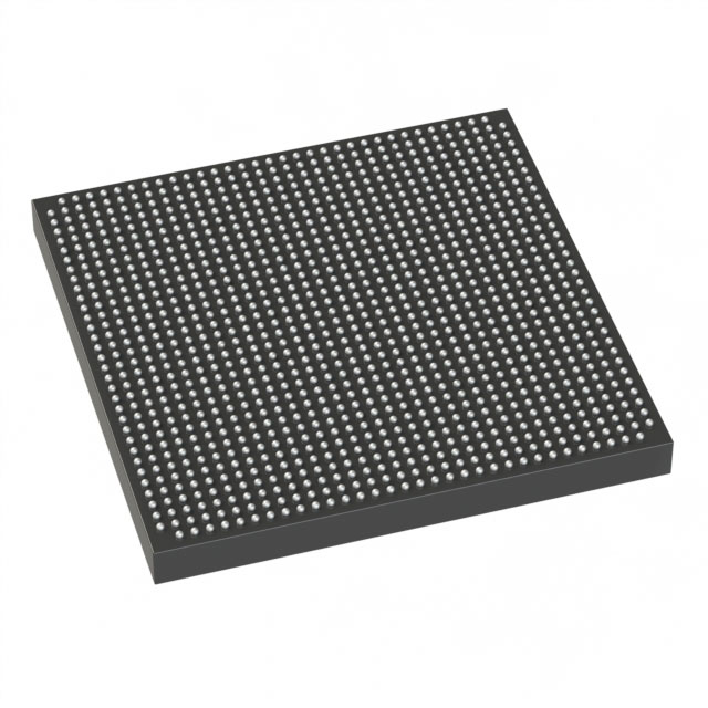
Stratix® III E Field Programmable Gate Array (FPGA) IC 744 8936448 107500 1152-BBGA, FCBGA |
|---|---|
| Quantity | 1,208 Available (as of June 10, 2026) |

| Product Category | Field Programmable Gate Array (FPGA) |
|---|---|
| Manufacturer | Intel |
| Manufacturing Status | Obsolete |
| Manufacturer Standard Lead Time | Contact Us |
| Datasheet |
Specifications & Environmental
| Device Package | 1152-FBGA (35x35) | Grade | Commercial | Operating Temperature | 0°C – 85°C | ||
|---|---|---|---|---|---|---|---|
| Package / Case | 1152-BBGA, FCBGA | Number of I/O | 744 | Voltage | 860 mV - 1.15 V | ||
| Mounting Method | Surface Mount | RoHS Compliance | RoHS Compliant | REACH Compliance | REACH Unknown | ||
| Moisture Sensitivity Level | 3 (168 Hours) | Number of LABs/CLBs | 4300 | Number of Logic Elements/Cells | 107500 | ||
| Number of Gates | N/A | ECCN | 3A001A7A | HTS Code | 8542.39.0001 | ||
| Qualification | N/A | Total RAM Bits | 8936448 |
Overview of EP3SE110F1152C3N – Stratix® III E Field Programmable Gate Array (FPGA) IC
The EP3SE110F1152C3N is a Stratix® III E family FPGA IC from Intel, designed for high-capacity, reprogrammable logic implementations. It combines a large logic fabric with abundant I/O and on‑chip memory to support complex digital designs and high‑speed interface applications.
Built on the Stratix III architecture, this device targets applications that require significant logic resources, dense I/O counts, embedded memory, and configurable I/O and system features while operating within commercial temperature and voltage ranges.
Key Features
- Logic Capacity — 107,500 logic elements and 4,300 logic array blocks (LABs) provide substantial programmable resources for complex logic and control functions.
- Embedded Memory — Approximately 8.9 Mbits of on‑chip RAM (8,936,448 total RAM bits) for buffers, FIFOs, and local storage.
- High I/O Count — 744 I/O pins to support wide parallel interfaces and multiple high‑speed links.
- DSP and Timing Resources — Stratix III family architecture includes DSP blocks, PLLs, and dedicated clock networks for timing and signal processing (as described in the device handbook).
- High‑Speed I/O and External Memory Interfaces — Series features cover high‑speed differential I/O with DPA and multiple external memory interface options (as documented in the Stratix III device handbook).
- Configuration and Test — Support for configuration and remote system upgrades plus IEEE 1149.1 (JTAG) boundary‑scan testing per device handbook guidance.
- Power and Supply — Core supply range from 860 mV to 1.15 V to match Stratix III E core voltage requirements.
- Package and Mounting — 1152‑BBGA FCBGA package; supplier device package listed as 1152‑FBGA (35×35). Surface mount mounting type.
- Operating Conditions — Commercial grade operation with an operating temperature range of 0 °C to 85 °C.
- RoHS Compliant — Device listed as RoHS compliant.
Typical Applications
- High‑density logic systems — Implement large custom digital functions and control logic using the device’s 107,500 logic elements and 4,300 LABs.
- Memory interface controllers — Use the device’s embedded memory (approximately 8.9 Mbits) alongside external memory interface capabilities for buffering and data path control.
- High‑I/O communication endpoints — Support multi‑lane and parallel interfaces with 744 available I/O pins and the Stratix III family’s high‑speed I/O features.
Unique Advantages
- Large programmable fabric: 107,500 logic elements enable implementation of complex algorithms and wide datapaths without immediate need for external logic.
- Substantial on‑chip memory: Approximately 8.9 Mbits of embedded RAM reduces dependence on external memory for many buffering and temporary storage tasks.
- Extensive I/O resources: 744 I/Os permit flexible partitioning of interfaces and simultaneous support for multiple peripherals and protocols.
- Configurable I/O and timing: Family‑level features such as DSP blocks, PLLs, and clock networks (documented in the device handbook) assist in building synchronous, high‑performance systems.
- Commercial deployment ready: Commercial temperature range (0 °C to 85 °C) and RoHS compliance support mainstream product designs and regulatory requirements.
- Compact surface‑mount package: 1152‑BBGA FCBGA (1152‑FBGA, 35×35) provides a high‑density board footprint for space‑constrained designs.
Why Choose EP3SE110F1152C3N?
The EP3SE110F1152C3N delivers a balanced combination of large logic capacity, significant embedded memory, and a high I/O count in a compact FCBGA package. It is appropriate for engineering teams building complex digital systems that require flexible, reprogrammable hardware and robust interface support within commercial operating conditions.
As a member of the Stratix III family, this device aligns with the documented architecture elements—memory blocks, DSP resources, clocking structures, and configuration options—documented in the Stratix III device handbook, providing predictable integration into FPGA‑based designs.
Request a quote or submit an inquiry to obtain pricing, availability, and ordering information for EP3SE110F1152C3N.


Date Founded: 1968
Headquarters: Santa Clara, California, USA
Employees: 130,000+
Revenue: $54.23 Billion
Certifications and Memberships: ISO9001:2015, ISO14001:2015, ISO17025:2017, ISO27001:2022, ISO45001:2018, ISO50001:2018


