
EP3SE260F1152C2G
| Part Description |
Field Programmable Gate Array (FPGA) IC |
|---|---|
| Quantity | 147 Available (as of June 15, 2026) |

| Product Category | Field Programmable Gate Array (FPGA) |
|---|---|
| Manufacturer | Intel |
| Manufacturing Status | Active |
| Manufacturer Standard Lead Time | 26 Weeks |
| Datasheet |
Specifications & Environmental
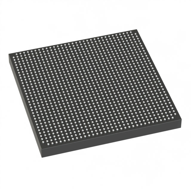
| Device Package | 1152-FBGA (35x35) | Grade | Commercial | Operating Temperature | 0°C – 85°C | ||
|---|---|---|---|---|---|---|---|
| Package / Case | 1152-BBGA, FCBGA | Number of I/O | 744 | Voltage | 860 mV - 1.15 V | ||
| Mounting Method | Surface Mount | RoHS Compliance | RoHS Compliant | REACH Compliance | REACH Unaffected | ||
| Moisture Sensitivity Level | 3 (168 Hours) | Number of LABs/CLBs | 10200 | Number of Logic Elements/Cells | 255000 | ||
| Number of Gates | N/A | ECCN | N/A | HTS Code | N/A | ||
| Qualification | N/A | Total RAM Bits | 16672768 |
Overview of EP3SE260F1152C2G – Field Programmable Gate Array (FPGA) IC
The EP3SE260F1152C2G is an Intel Stratix III family FPGA optimized for high-performance logic, digital signal processing (DSP), and embedded designs. It combines a large logic capacity with substantial on-chip memory and abundant I/O to support complex system integration in commercial applications.
Designed for applications that require programmable high-speed interfaces, flexible clocking and processing resources, this device targets communications, networking, memory interface controllers, and compute-accelerated systems where performance, integration and configurability matter.
Key Features
- Logic Capacity — 255,000 logic elements to implement complex logic and control functions.
- Embedded Memory — Approximately 16.7 Mbits of on-chip RAM (16,672,768 bits) for FIFOs, buffers and local storage.
- High I/O Count — 744 user I/O pins arranged for flexible interfacing and multi-bank I/O topologies.
- DSP & Arithmetic Resources — Stratix III architecture provides dedicated DSP multiplier resources and support for high-performance arithmetic (family-level DSP multiplier options documented in the device handbook).
- Clocking and PLLs — Multiple global, regional and peripheral clocks with up to 12 phase-locked loops per device for clock synthesis, switchover and dynamic phase control (family-level capability).
- Power and Core Voltage — Programmable power optimizations with a supported core supply range of 0.86 V to 1.15 V enabling selectable core voltage operation.
- Package and Mounting — 1152‑FBGA (35×35) FCBGA package; surface-mount mounting for standard PCB assembly.
- Operating Range — Commercial grade operation from 0 °C to 85 °C.
- Reliability and Security — Family-level features include configuration memory CRC and optional AES encryption for bitstream protection, plus ECC support for embedded memory blocks.
- Standards and Compliance — RoHS compliant.
Typical Applications
- High-performance DSP and compute — Use the device’s large logic fabric and on-chip memory for FIR filters, signal chains and acceleration of compute kernels.
- Networking and communications — Implement protocol engines, SERDES interfaces and multi-bank I/O for packet processing and high-speed link handling.
- Memory interface controllers — Leverage abundant I/O and dedicated memory support for DDR/DDR2/DDR3 and other external memory interfaces.
- Embedded systems and IP integration — Integrate soft processors and megafunction IP for control, offload and system orchestration.
Unique Advantages
- High logic density: 255,000 logic elements allow consolidation of complex functions into a single device, reducing board-level BOM and interconnect.
- Substantial on-chip memory: Approximately 16.7 Mbits of embedded RAM supports large buffers, FIFOs and state storage without external memory.
- Flexible clocking and PLLs: Multiple clock domains and up to 12 PLLs enable complex timing architectures and dynamic clock management.
- Selectable core voltage and power optimization: Core supply range of 0.86–1.15 V and programmable power technology support tuning for performance versus power trade-offs.
- Security and data integrity: Family-level support for AES encryption options and configuration CRC/ECC improves IP protection and runtime reliability.
- Rich I/O and package options: 744 user I/Os in a 1152-FBGA (35×35) surface-mount package provide broad system interfacing capability in a compact footprint.
Why Choose EP3SE260F1152C2G?
The EP3SE260F1152C2G positions itself as a high-capacity Stratix III FPGA option for commercial designs that need a balance of large logic resources, significant embedded memory and extensive I/O. It is suited to engineers implementing high-performance DSP, memory controllers and complex protocol logic who require configurable power and clocking options.
With family-level features such as advanced clocking, DSP multipliers, configuration security and ECC for memory, this device supports scalable designs and integration with existing FPGA IP and development flows. RoHS compliance and a standard surface-mount FBGA package simplify manufacturing and regulatory handling for commercial deployments.
Request a quote or submit an inquiry to receive pricing and availability information for EP3SE260F1152C2G.


Date Founded: 1968
Headquarters: Santa Clara, California, USA
Employees: 130,000+
Revenue: $54.23 Billion
Certifications and Memberships: ISO9001:2015, ISO14001:2015, ISO17025:2017, ISO27001:2022, ISO45001:2018, ISO50001:2018


