
EP3SE260F1152C3N
| Part Description |
Stratix® III E Field Programmable Gate Array (FPGA) IC 744 16672768 255000 1152-BBGA, FCBGA |
|---|---|
| Quantity | 1,147 Available (as of June 9, 2026) |

| Product Category | Field Programmable Gate Array (FPGA) |
|---|---|
| Manufacturer | Intel |
| Manufacturing Status | Obsolete |
| Manufacturer Standard Lead Time | Contact Us |
| Datasheet |
Specifications & Environmental
| Device Package | 1152-FBGA (35x35) | Grade | Commercial | Operating Temperature | 0°C – 85°C | ||
|---|---|---|---|---|---|---|---|
| Package / Case | 1152-BBGA, FCBGA | Number of I/O | 744 | Voltage | 860 mV - 1.15 V | ||
| Mounting Method | Surface Mount | RoHS Compliance | RoHS Compliant | REACH Compliance | REACH Unknown | ||
| Moisture Sensitivity Level | 3 (168 Hours) | Number of LABs/CLBs | 10200 | Number of Logic Elements/Cells | 255000 | ||
| Number of Gates | N/A | ECCN | 3A001A7A | HTS Code | 8542.39.0001 | ||
| Qualification | N/A | Total RAM Bits | 16672768 |
Overview of EP3SE260F1152C3N – Stratix® III E FPGA, 255,000 logic elements, 744 I/O, 1152-BBGA
The EP3SE260F1152C3N is a Stratix® III E field programmable gate array (FPGA) IC from Intel, designed for high-density, configurable digital logic integration. Built on the Stratix III device family architecture, the device combines a large logic resource pool with extensive on-chip memory and flexible I/O to support complex system designs.
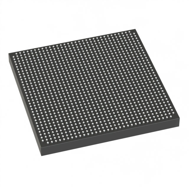
This 1152-BBGA, surface-mount FPGA provides 255,000 logic elements, approximately 16.7 Mbits of embedded memory, and 744 I/O pins, making it suitable for applications that require dense logic implementation, substantial embedded RAM, and wide external interfacing. The device operates over a core supply range of 860 mV to 1.15 V and is rated for commercial temperature operation from 0 °C to 85 °C.
Key Features
- Logic Capacity — 255,000 logic elements provide a high-density programmable fabric for complex combinational and sequential logic implementation.
- Embedded Memory — Approximately 16.7 Mbits of on-chip RAM delivered via TriMatrix embedded memory blocks for buffering, FIFOs, and intermediate data storage.
- I/O and Interfaces — 744 user I/O pins in a 1152-BBGA (35 × 35) FCBGA package support broad external connectivity, including support for high-speed differential I/O interfaces with DPA as described in the device family handbook.
- DSP and Signal Processing — Integrated DSP blocks from the Stratix III family provide hardware resources tailored for arithmetic and signal-processing functions.
- Clocking and PLLs — Advanced clock networks and PLL resources support flexible clock distribution and multiple clock domains.
- Configuration and Test — Family features include remote system upgrade capability and IEEE 1149.1 (JTAG) boundary-scan testing for programming and debug workflows.
- Power and Voltage — Core voltage range of 860 mV to 1.15 V with programmable power options referenced in the device handbook for power management strategies.
- Package and Mounting — 1152-BBGA (1152-FBGA, 35 × 35) surface-mount package suitable for compact, board-level integration; RoHS compliant.
- System Reliability and Security — Device-family features include design security, SEU mitigation options, and programmable power controls to support robust system behavior.
Typical Applications
- High-density signal processing — Use the device's DSP blocks and large logic element count to implement filtering, transforms, and real-time processing pipelines.
- External memory controllers and data buffering — The combination of abundant on-chip RAM and extensive I/O supports high-throughput interfaces to external memory and buffering architectures.
- High-speed serial and parallel interfaces — 744 I/O and the Stratix III family’s high-speed differential I/O features enable implementation of wide buses and differential link endpoints.
- Configurable system integration — Leverage remote upgrade capability and JTAG boundary-scan for in-system programming, debug, and field updates of complex FPGA-based subsystems.
Unique Advantages
- High logic density: 255,000 logic elements let you consolidate large functions into a single device, reducing board count and simplifying routing.
- Substantial on-chip memory: Approximately 16.7 Mbits of embedded RAM minimizes dependence on external memory for many buffering and storage tasks.
- Extensive I/O availability: 744 I/O pins in a compact 1152-BBGA package provide flexible connectivity for multi-channel systems and wide external interfaces.
- Integrated signal-processing resources: DSP blocks and advanced clocking resources accelerate arithmetic-heavy workloads and reduce the need for external accelerators.
- Commercial-grade operating range: Rated for 0 °C to 85 °C, supporting a wide range of commercial embedded applications and deployments.
- Standards-based test and configuration: JTAG boundary-scan and remote upgrade capabilities streamline manufacturing test, programming, and field maintenance.
Why Choose EP3SE260F1152C3N?
The EP3SE260F1152C3N positions itself as a high-density, highly configurable FPGA option within the Stratix III family, offering a balance of large logic resources, significant embedded memory, and extensive I/O in a single surface-mount 1152-BBGA package. Its on-chip DSP resources, advanced clocking, and device-family reliability features make it well suited for demanding embedded designs that require integrated processing and broad external interfacing.
Designed and supplied by Intel as part of the Stratix III family, this device is appropriate for teams implementing complex digital systems that benefit from scalable logic capacity, on-chip RAM, and configurable I/O while leveraging device-family configuration and test features for development and production workflows.
Request a quote or submit an inquiry to get pricing and availability information for EP3SE260F1152C3N and to discuss your design requirements with a product specialist.


Date Founded: 1968
Headquarters: Santa Clara, California, USA
Employees: 130,000+
Revenue: $54.23 Billion
Certifications and Memberships: ISO9001:2015, ISO14001:2015, ISO17025:2017, ISO27001:2022, ISO45001:2018, ISO50001:2018


