
EP3SE260F1517C4LN
| Part Description |
Stratix® III E Field Programmable Gate Array (FPGA) IC 976 16672768 255000 1517-BBGA, FCBGA |
|---|---|
| Quantity | 582 Available (as of June 10, 2026) |

| Product Category | Field Programmable Gate Array (FPGA) |
|---|---|
| Manufacturer | Intel |
| Manufacturing Status | Obsolete |
| Manufacturer Standard Lead Time | Contact Us |
| Datasheet |
Specifications & Environmental
| Device Package | 1517-FBGA (40x40) | Grade | Commercial | Operating Temperature | 0°C – 85°C | ||
|---|---|---|---|---|---|---|---|
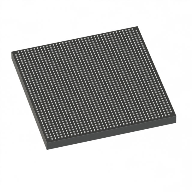
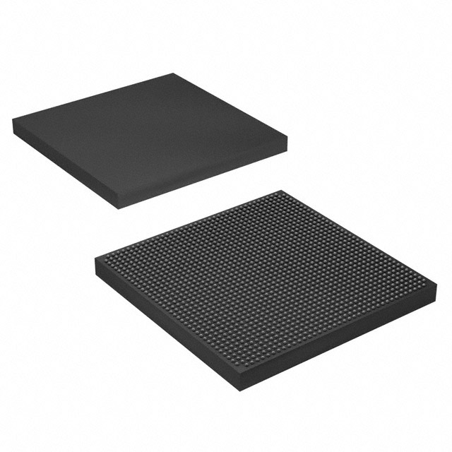
| Package / Case | 1517-BBGA, FCBGA | Number of I/O | 976 | Voltage | 860 mV - 1.15 V | ||
| Mounting Method | Surface Mount | RoHS Compliance | RoHS Compliant | REACH Compliance | REACH Unknown | ||
| Moisture Sensitivity Level | 3 (168 Hours) | Number of LABs/CLBs | 10200 | Number of Logic Elements/Cells | 255000 | ||
| Number of Gates | N/A | ECCN | 3A001A2C | HTS Code | 8542.39.0001 | ||
| Qualification | N/A | Total RAM Bits | 16672768 |
Overview of EP3SE260F1517C4LN – Stratix® III E Field Programmable Gate Array (FPGA)
The EP3SE260F1517C4LN is a commercial-grade Stratix® III E field programmable gate array (FPGA) from Intel, designed for high-density, board-mounted digital designs. It combines a large logic capacity and substantial embedded memory with a high pin count and a compact 1517-BBGA (40×40 FCBGA) package for surface-mount applications.
Targeted at commercial applications, this device offers a balance of integration and scalability for complex digital processing, interface bridging, and system-level prototyping where high logic density and significant on-chip RAM are required.
Key Features
- Logic Capacity — 255,000 logic elements provide the programmable resources required for complex digital functions and custom logic implementations.
- Embedded Memory — Approximately 16.7 Mbits of on-chip RAM to implement buffers, FIFOs, and distributed memory structures without external RAM.
- I/O Density — 976 general-purpose I/O pins to support wide parallel buses, multiple high-pin-count interfaces, and extensive signal routing on the board.
- Power Supply Range — Core voltage supply from 0.860 V to 1.15 V to match system power architectures and regulator choices.
- Package & Mounting — 1517-BBGA (1517-FBGA, 40×40) package for surface-mount PCB assembly, enabling compact board layouts and high pin density.
- Operating Range & Grade — Commercial-grade device rated for operation from 0 °C to 85 °C, suitable for business, consumer, and many industrial-adjacent electronics environments.
- Regulatory Compliance — RoHS compliant, supporting lead-free assembly and environmentally conscious designs.
Typical Applications
- High-density digital processing: Use the 255,000 logic elements and ~16.7 Mbits of embedded memory to implement complex signal processing, protocol handling, and custom compute blocks on a single device.
- Interface aggregation and bridging: Leverage 976 I/O pins to connect multiple parallel buses, translate between protocols, or aggregate high-pin-count peripherals.
- System prototypes and product development: Compact 1517-BBGA surface-mount package and broad logic capacity make this FPGA suitable for development boards and pre-production hardware.
Unique Advantages
- High programmable density: Large logic element count enables consolidation of multiple functions into a single FPGA, reducing board-level BOM and interconnect complexity.
- Substantial on-chip memory: Approximately 16.7 Mbits of embedded RAM reduce dependence on external memory components and simplify timing and PCB routing.
- Extensive external connectivity: Nearly 1,000 I/O pins permit flexible system I/O assignment and support for multiple parallel interfaces without external multiplexing.
- Compact, board-friendly package: 1517-BBGA (40×40 FCBGA) surface-mount footprint helps maximize routing density while keeping the overall PCB area manageable.
- Commercial-grade operating range: Rated 0 °C to 85 °C for reliable operation across typical commercial environments and product deployments.
- RoHS compliant: Supports lead-free manufacturing and environmental compliance goals.
Why Choose EP3SE260F1517C4LN?
The EP3SE260F1517C4LN positions itself as a high-capacity, commercially graded FPGA option for designs that require substantial programmable logic, on-chip memory, and extensive I/O in a compact surface-mount package. Its combination of 255,000 logic elements, approximately 16.7 Mbits of embedded RAM, and 976 I/Os delivers a platform capable of consolidating complex system functions and reducing external component count.
This device is well suited for engineering teams and OEMs building advanced digital systems, interface-heavy boards, or prototype platforms that benefit from a scalable FPGA architecture, compact 1517-BBGA footprint, and RoHS compliance for streamlined manufacturing.
Request a quote or contact sales to check pricing, availability, and lead times for the EP3SE260F1517C4LN. Provide your quantity and delivery requirements to receive a tailored response.


Date Founded: 1968
Headquarters: Santa Clara, California, USA
Employees: 130,000+
Revenue: $54.23 Billion
Certifications and Memberships: ISO9001:2015, ISO14001:2015, ISO17025:2017, ISO27001:2022, ISO45001:2018, ISO50001:2018


