
EP3SE50F484C2
| Part Description |
Stratix® III E Field Programmable Gate Array (FPGA) IC 296 5760000 47500 484-BBGA, FCBGA |
|---|---|
| Quantity | 1,285 Available (as of June 15, 2026) |
| Product Category | Field Programmable Gate Array (FPGA) |
|---|---|
| Manufacturer | Intel |
| Manufacturing Status | Obsolete |
| Manufacturer Standard Lead Time | Contact Us |
| Datasheet |
Specifications & Environmental
| Device Package | 484-FBGA (23x23) | Grade | Commercial | Operating Temperature | 0°C – 85°C | ||
|---|---|---|---|---|---|---|---|
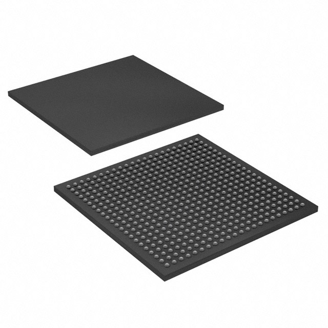
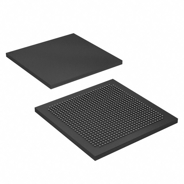
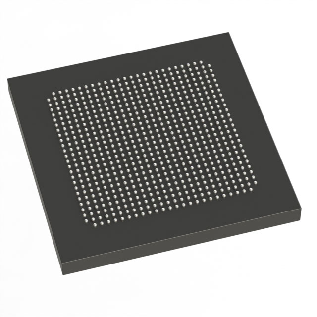
| Package / Case | 484-BBGA, FCBGA | Number of I/O | 296 | Voltage | 860 mV - 1.15 V | ||
| Mounting Method | Surface Mount | RoHS Compliance | RoHS Compliant | REACH Compliance | REACH Unknown | ||
| Moisture Sensitivity Level | 3 (168 Hours) | Number of LABs/CLBs | 1900 | Number of Logic Elements/Cells | 47500 | ||
| Number of Gates | N/A | ECCN | 3A001A2C | HTS Code | 8542.39.0001 | ||
| Qualification | N/A | Total RAM Bits | 5760000 |
Overview of EP3SE50F484C2 – Stratix® III E Field Programmable Gate Array (FPGA) IC 296 I/O, ~5.76 Mbits RAM, 47,500 logic elements, 484-BBGA
The EP3SE50F484C2 is an Intel Stratix® III E Field Programmable Gate Array (FPGA) in a 484-ball BGA (FCBGA) package. It provides a high-density programmable fabric with 47,500 logic elements, approximately 5.76 Mbits of embedded memory and 296 user I/O to support complex digital designs.
Designed for commercial-grade systems, this device combines significant logic and on-chip memory capacity with a compact surface-mount 484-FBGA (23×23) package and a low-voltage core supply range, making it suitable for logic- and I/O-intensive applications within the 0 °C to 85 °C operating range.
Key Features
- Core Logic — 47,500 logic elements provide substantial programmable logic capacity for complex logic functions and system integration.
- Embedded Memory — Approximately 5.76 Mbits of on-chip RAM to support buffers, FIFOs, and intermediate data storage without external memory.
- I/O Capability — 296 user I/O pins allow dense interfacing to external devices, peripherals, and high-pin-count boards.
- Package — 484-ball BGA package (484-FBGA, 23×23) in FCBGA format enables surface-mount assembly and compact board integration.
- Power — Core voltage supply range from 860 mV to 1.15 V to match system power architectures and support low-voltage operation.
- Thermal/Grade — Commercial temperature grade with an operating range of 0 °C to 85 °C.
- Mounting — Surface-mount device for standard PCB assembly processes.
- Environmental — RoHS-compliant for regulatory and supply-chain compatibility.
Typical Applications
- Communications Equipment — Implements packet processing, protocol bridging, and custom logic where high logic density and many I/O are needed.
- Video and Signal Processing — Provides on-chip RAM and abundant logic resources for buffering, real-time processing, and data routing tasks.
- Test & Measurement — Enables custom timing, data acquisition, and instrument control with flexible I/O and programmable logic.
- System Prototyping — Acts as a configurable platform for validating hardware architectures that require significant logic capacity and numerous I/O connections.
Unique Advantages
- High Logic Density: 47,500 logic elements accommodate complex state machines, datapaths, and custom accelerators without excessive board-level partitioning.
- Substantial On-Chip Memory: Approximately 5.76 Mbits of embedded RAM reduces dependence on external memory for temporary storage and buffering.
- Extensive I/O Count: 296 I/O pins support high-connectivity designs, simplifying routing to peripherals and external components.
- Compact BGA Package: 484-FBGA (23×23) FCBGA footprint provides a balance of density and manufacturability for space-constrained PCBs.
- Low-Voltage Core: 860 mV to 1.15 V supply range aligns with modern low-voltage power domains to help manage system power budgets.
- Commercial-Grade and RoHS-Compliant: Rated for 0 °C to 85 °C operation and RoHS compliance for broad commercial deployment and environmental compliance.
Why Choose EP3SE50F484C2?
The EP3SE50F484C2 delivers a combination of high logic capacity, significant embedded memory, and a large number of I/O in a compact 484-ball FCBGA package—positioning it for commercial designs that require dense programmable logic and flexible system interfacing. Its low-voltage core and surface-mount packaging make it suitable for modern PCB power and assembly flows.
This device is well suited to engineering teams building communications gear, signal-processing platforms, test equipment, or hardware prototypes that need on-chip memory, extensive I/O, and a sizable logic fabric. Its specification set offers a clear pathway for scalable, robust designs within commercial temperature limits.
Request a quote or submit an inquiry to obtain pricing and availability for the EP3SE50F484C2 and to discuss how it can fit into your next design.


Date Founded: 1968
Headquarters: Santa Clara, California, USA
Employees: 130,000+
Revenue: $54.23 Billion
Certifications and Memberships: ISO9001:2015, ISO14001:2015, ISO17025:2017, ISO27001:2022, ISO45001:2018, ISO50001:2018


