
EP3SE50F484I4G
| Part Description |
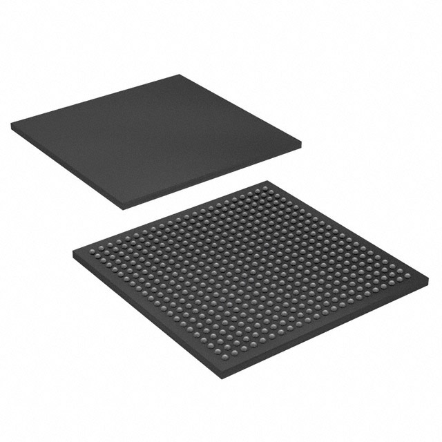
Stratix® III E Field Programmable Gate Array (FPGA) IC 296 5760000 47500 484-BBGA, FCBGA |
|---|---|
| Quantity | 586 Available (as of June 15, 2026) |

| Product Category | Field Programmable Gate Array (FPGA) |
|---|---|
| Manufacturer | Intel |
| Manufacturing Status | Active |
| Manufacturer Standard Lead Time | 26 Weeks |
| Datasheet |
Specifications & Environmental
| Device Package | 484-FBGA (23x23) | Grade | Industrial | Operating Temperature | -40°C – 100°C | ||
|---|---|---|---|---|---|---|---|
| Package / Case | 484-BBGA, FCBGA | Number of I/O | 296 | Voltage | 860 mV - 1.15 V | ||
| Mounting Method | Surface Mount | RoHS Compliance | RoHS Compliant | REACH Compliance | REACH Unaffected | ||
| Moisture Sensitivity Level | 3 (168 Hours) | Number of LABs/CLBs | 1900 | Number of Logic Elements/Cells | 47500 | ||
| Number of Gates | N/A | ECCN | PENDING ECCN | HTS Code | 0000.00.0000 | ||
| Qualification | N/A | Total RAM Bits | 5760000 |
Overview of EP3SE50F484I4G – Stratix® III E FPGA, 484-BBGA (Industrial)
The EP3SE50F484I4G is an Intel Stratix® III E field-programmable gate array (FPGA) in a 484-BBGA FCBGA package targeted at memory- and multiplier-rich, data-centric applications. It combines a high logic capacity with significant on-chip memory and dedicated DSP resources for demanding signal processing, packet processing, and high‑speed interface designs.
This industrial-grade device supports a wide operating temperature range and a selectable core voltage window, enabling deployment in systems that require sustained performance across harsh environments while providing power-management flexibility.
Key Features
- Logic Capacity 47,500 logic elements provide substantial programmable logic resources for complex state machines, control logic, and custom datapaths.
- Embedded Memory Approximately 5.76 Mbits of on-chip RAM to implement buffers, FIFOs, and intermediate storage; family architectures support TriMatrix memory for flexible dual-port memory implementations.
- High‑Performance DSP Dedicated DSP/multiplier structures in the Stratix III family support a range of multiplier sizes and multiply-accumulate functions for real-time signal processing and acceleration tasks.
- I/O and High‑Speed Interfaces 296 user I/O pins with support for dynamic on-chip termination, high-speed differential signaling, serializer/deserializer (SERDES) functions and dynamic phase alignment for robust high-speed links.
- Clocking and PLLs Multiple global, regional, and peripheral clocks with up to 12 PLLs per device (family-level) enable complex clocking schemes and clock synthesis for multi-rate designs.
- Power Management Selectable core voltage and Programmable Power Technology (family-level) provide granular control over performance versus power consumption; device core operates within a 0.86 V to 1.15 V supply range.
- Security and Reliability Family-level support for 256-bit AES configuration encryption plus built-in CRC and ECC circuitry help protect configuration and user memory against corruption and soft errors.
- Package and Thermal 484-BBGA (484-FBGA, 23×23) surface-mount package; rated for industrial operation from −40°C to 100°C.
Typical Applications
- High‑performance DSP systems Use the device’s dedicated multipliers and on-chip memory for FIR filters, FFTs, and other real-time signal-processing pipelines.
- High‑speed memory controllers Implement DDR/DDR2/DDR3 and other external-memory interfaces using the device’s modular I/O banks and dedicated DQS logic (family-level support detailed in the Stratix III handbook).
- Network and communications equipment Build packet processors, line cards, and protocol bridges leveraging high-speed differential I/O, SERDES, and dynamic phase alignment.
- Embedded compute and control Integrate custom logic, interface handling, and embedded processors for industrial control, instrumentation, and measurement systems.
Unique Advantages
- Substantial programmable logic 47,500 logic elements let you consolidate functions into a single FPGA, reducing component count and board complexity.
- Significant on‑chip RAM Approximately 5.76 Mbits of embedded memory supports deep buffering and high-throughput data paths without relying solely on external memory.
- Dedicated DSP resources On-chip multipliers and DSP blocks accelerate math-intensive workloads and offload processing from general-purpose processors.
- Industrial temperature rating −40°C to 100°C operating range allows deployment in temperature‑challenging environments common in industrial applications.
- Flexible power/performance trade-offs Selectable core voltage and programmable power features allow designers to tune device behavior for performance or energy efficiency.
- Robust configuration and data integrity Family-level AES encryption, CRC, and ECC support add layers of protection for configuration and user data, improving system reliability.
Why Choose EP3SE50F484I4G?
The EP3SE50F484I4G places a balanced combination of logic, embedded memory, and DSP capability into a compact 484-BBGA industrial package. It is well suited for designers building data-centric systems that require substantial on-chip resources, flexible high-speed I/O, and configurable power/performance trade-offs.
For engineering teams targeting industrial communications, signal processing, or memory‑intensive applications, this Stratix III E device offers a proven family architecture with features aimed at integration, reliability, and performance scalability.
Request a quote or submit a request for pricing and availability to receive product and purchasing details tailored to your project needs.


Date Founded: 1968
Headquarters: Santa Clara, California, USA
Employees: 130,000+
Revenue: $54.23 Billion
Certifications and Memberships: ISO9001:2015, ISO14001:2015, ISO17025:2017, ISO27001:2022, ISO45001:2018, ISO50001:2018


