
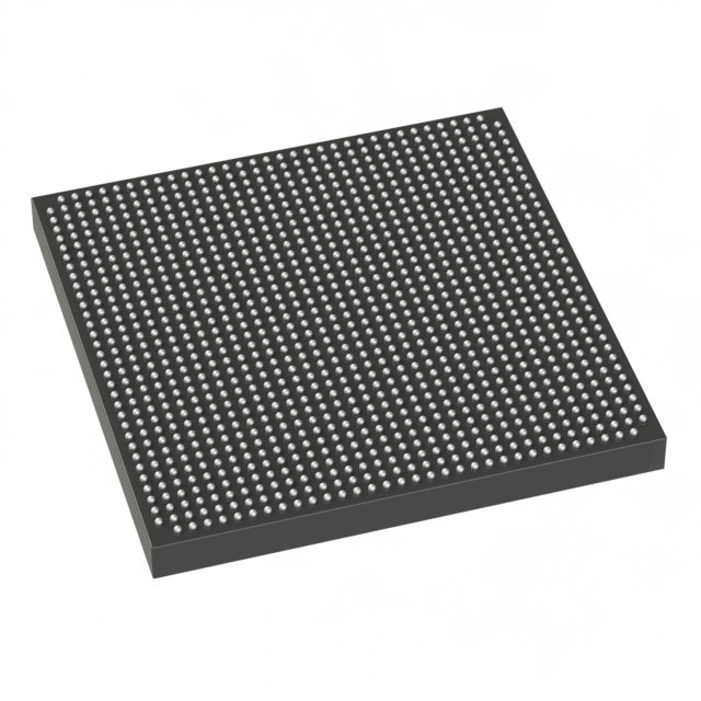
EP3SE80F1152C3G
| Part Description |
Field Programmable Gate Array (FPGA) IC |
|---|---|
| Quantity | 889 Available (as of October 8, 2026) |

| Product Category | Field Programmable Gate Array (FPGA) |
|---|---|
| Manufacturer | Intel |
| Manufacturing Status | Active |
| Manufacturer Standard Lead Time | 26 Weeks |
| Datasheet |
Specifications & Environmental
| Device Package | 1152-FBGA (35x35) | Grade | Commercial | Operating Temperature | 0°C – 85°C | ||
|---|---|---|---|---|---|---|---|
| Package / Case | 1152-BBGA, FCBGA | Number of I/O | 744 | Voltage | 860 mV - 1.15 V | ||
| Mounting Method | Surface Mount | RoHS Compliance | RoHS Compliant | REACH Compliance | REACH Unaffected | ||
| Moisture Sensitivity Level | 3 (168 Hours) | Number of LABs/CLBs | 3200 | Number of Logic Elements/Cells | 80000 | ||
| Number of Gates | N/A | ECCN | N/A | HTS Code | N/A | ||
| Qualification | N/A | Total RAM Bits | 6843392 |
Overview of EP3SE80F1152C3G – Field Programmable Gate Array (FPGA) IC
The EP3SE80F1152C3G is a Stratix III family FPGA offering a high-density, programmable logic platform for computation- and interface-intensive designs. Built for high-performance logic, DSP and embedded applications, this device combines 80,000 logic elements with substantial on-chip memory and a wide complement of I/O to support complex system integration.
Designed for commercial applications, the device provides flexible power and clocking options, advanced on-chip reliability and security features from the Stratix III family, and a compact 1152‑FBGA package for surface-mount assembly.
Key Features
- Logic Capacity — 80,000 logic elements to implement complex state machines, custom datapaths and control logic.
- Embedded Memory — Approximately 6.84 Mbits of on-chip RAM (TriMatrix family memory architecture) for buffers, FIFOs and local storage.
- High‑Density I/O — 744 user I/O pins to support multiple external interfaces and parallel bus connections.
- Core Power and Process — Selectable core voltage operation with device supply range of 0.860 V to 1.15 V, based on the Stratix III 65 nm process and programmable power technology.
- Clocking and PLLs — Family-level support includes multiple global and regional clocks and up to 12 PLLs for flexible clock synthesis and phase control.
- High‑Speed I/O and SERDES — Stratix III family features include SERDES and dynamic phase alignment circuitry supporting high-speed differential I/O (family-stated up to 1.6 Gbps).
- Security and Reliability — Family features include optional 256-bit AES configuration bitstream security and on-chip CRC/ECC circuitry for configuration and memory error detection/correction.
- Package and Mounting — 1152-FBGA (35 × 35 mm) package, surface-mount, commercial grade with operating range 0 °C to 85 °C.
- Standards and IP Support — Stratix III family supports the Nios II embedded processor and Altera MegaCore IP megafunctions for common interfaces and functions.
- Compliance — RoHS compliant.
Typical Applications
- High‑Performance DSP and Signal Processing — Use the device’s logic density, embedded memory and family DSP capabilities to implement filters, FFTs and real-time signal chains.
- Networking and Communications — Leverage high-speed differential I/O and SERDES support for protocol bridging, packet processing and interface aggregation.
- Memory Interface Controllers — Implement DDR/DDR2/DDR3 or other external memory controllers with available I/O and dedicated memory interface features from the Stratix III family.
- Embedded Systems and Acceleration — Deploy as an application-specific accelerator or as the central programmable logic element in embedded platforms that benefit from reconfiguration and custom datapaths.
Unique Advantages
- Highly integrated resource set: 80,000 logic elements combined with ~6.84 Mbits of embedded memory and 744 I/Os reduce external components and simplify board-level design.
- Flexible power/performance trade-offs: Selectable core voltage (0.860–1.15 V) and Stratix III programmable power technology enable tuning between lower power and higher performance modes.
- Built-in security and reliability: Family-level support for 256-bit AES configuration security and CRC/ECC protection helps safeguard IP and improves runtime robustness.
- Rich clocking and timing control: Extensive clocking resources and up to 12 PLLs provide the timing flexibility required for multi‑domain and high‑speed designs.
- Proven IP and ecosystem: Support for Nios II and Altera MegaCore functions accelerates development with tested building blocks and software infrastructure.
- Commercial package and assembly: 1152‑FBGA surface-mount package in a compact 35 × 35 mm footprint supports dense board layouts for space-constrained systems.
Why Choose EP3SE80F1152C3G?
The EP3SE80F1152C3G positions itself as a capable, commercially graded Stratix III FPGA for customers requiring a balance of logic density, on-chip memory and high I/O count in a single-package solution. Its selectable core voltage and family-level power optimizations allow designers to tune devices for their target performance and power envelopes.
This device is well suited to teams building DSP-heavy, networking or embedded-accelerator systems that need reconfigurability, integrated security and robust clocking. Combined with available Stratix III IP and processor support, it provides a scalable platform for medium-to-high complexity designs with long-term maintainability.
Request a quote or submit an inquiry to receive pricing, lead-time and availability information for EP3SE80F1152C3G.























Date Founded: 1968
Headquarters: Santa Clara, California, USA
Employees: 130,000+
Revenue: $54.23 Billion
Certifications and Memberships: ISO9001:2015, ISO14001:2015, ISO17025:2017, ISO27001:2022, ISO45001:2018, ISO50001:2018


