
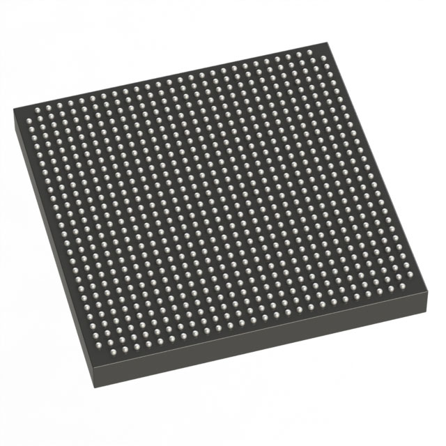
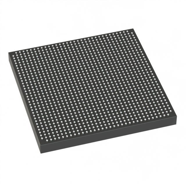
EP3SL110F780C2G
| Part Description |
Field Programmable Gate Array (FPGA) IC |
|---|---|
| Quantity | 177 Available (as of June 18, 2026) |

| Product Category | Field Programmable Gate Array (FPGA) |
|---|---|
| Manufacturer | Intel |
| Manufacturing Status | Active |
| Manufacturer Standard Lead Time | 26 Weeks |
| Datasheet |
Specifications & Environmental
| Device Package | 780-FBGA (29x29) | Grade | Commercial | Operating Temperature | 0°C – 85°C | ||
|---|---|---|---|---|---|---|---|
| Package / Case | 780-BBGA, FCBGA | Number of I/O | 488 | Voltage | 860 mV - 1.15 V | ||
| Mounting Method | Surface Mount | RoHS Compliance | RoHS Compliant | REACH Compliance | REACH Unaffected | ||
| Moisture Sensitivity Level | 3 (168 Hours) | Number of LABs/CLBs | 4300 | Number of Logic Elements/Cells | 107500 | ||
| Number of Gates | N/A | ECCN | N/A | HTS Code | N/A | ||
| Qualification | N/A | Total RAM Bits | 4992000 |
Overview of EP3SL110F780C2G – Field Programmable Gate Array (FPGA) IC
The EP3SL110F780C2G is an Intel Stratix III family FPGA supplied in a 780-ball FCBGA package for surface-mount applications. It provides high logic density and substantial on-chip memory for compute-intensive, signal-processing and embedded applications.
Built on the Stratix III architecture, the device emphasizes configurable performance and power tradeoffs through selectable core voltage and Programmable Power Technology, making it suitable for designs that require a balance of logic resources, memory, and high-speed I/O capability.
Key Features
- Logic Capacity Approximately 107,500 logic elements, enabling implementation of complex digital logic and control functions.
- On-Chip Memory Approximately 4.99 Mbits of embedded RAM for large FIFOs, buffers, and on-chip data storage.
- I/O Resources 488 user I/O pins in a modular bank structure suitable for diverse interface standards and board-level integration.
- DSP and Arithmetic Support Stratix III family DSP resources (family-level feature) support dedicated multipliers and multiply-accumulate functions for signal-processing workloads.
- Clocking and PLLs Family-level support for multiple global, regional, and peripheral clocks plus up to 12 PLLs for clock synthesis and phase control.
- Power and Voltage Selectable core operation with a specified supply range of 0.86 V to 1.15 V to balance performance and power consumption.
- Security and Reliability Family-level support for 256-bit AES encryption options and on-chip CRC/ECC features to detect and manage configuration and memory errors.
- Package and Mounting 780-ball FBGA (29×29) surface-mount package for compact, high-density board designs.
- Commercial Temperature Grade Rated for operation from 0 °C to 85 °C and specified as commercial grade for standard temperature-range applications.
- Regulatory RoHS compliant.
Typical Applications
- High-Performance Signal Processing Use the device’s logic density and family DSP resources to implement FIR filters, FFT engines, and other real-time signal-processing blocks.
- Embedded Systems and Control Leverage abundant logic elements and on-chip RAM for custom processors, protocol handling, and control-state machines.
- Memory Interface and Buffering Employ the embedded RAM and I/O bank structure for memory controllers, large FIFOs, and interface bridging between memory types.
- Networking and Communications Implement packet processing, protocol offload, and SERDES-capable I/O (family-level) for mid- to high-speed data links.
Unique Advantages
- High Logic Integration: Approximately 107,500 logic elements reduce the need for multiple discrete devices and simplify system architecture.
- Substantial Embedded Memory: Approximately 4.99 Mbits of on-chip RAM supports large buffers and high-throughput streaming without external memory dependence.
- Power/Performance Flexibility: Selectable core voltage and Programmable Power Technology allow designers to tune for lower power or higher performance as required by the application.
- Robust Clocking and DSP Support: Multiple clocks, PLLs, and family DSP resources enable complex timing architectures and efficient implementation of arithmetic-intensive tasks.
- Compact, Board-Friendly Package: 780-FBGA (29×29) surface-mount package provides a high-density solution for space-constrained boards.
- Commercial Temperature Suitability: Specified 0 °C to 85 °C operation for standard commercial applications and environments.
Why Choose EP3SL110F780C2G?
The EP3SL110F780C2G combines a high count of logic elements with several megabits of embedded RAM and a 780-ball FCBGA package to deliver a compact, capable FPGA for compute- and memory-intensive designs. Its selectable core voltage and family-level Programmable Power Technology provide practical options for optimizing power consumption without redesigning the hardware.
This device is suited for engineering teams developing signal-processing, embedded control, memory-interface, or communications products that require a commercial-temperature FPGA with substantial on-chip resources and family-provided features such as encryption and robust clocking.
Request a quote or submit a procurement inquiry to check availability and lead times for EP3SL110F780C2G.


Date Founded: 1968
Headquarters: Santa Clara, California, USA
Employees: 130,000+
Revenue: $54.23 Billion
Certifications and Memberships: ISO9001:2015, ISO14001:2015, ISO17025:2017, ISO27001:2022, ISO45001:2018, ISO50001:2018


