
EP3SL110F780C3G
| Part Description |
Field Programmable Gate Array (FPGA) IC |
|---|---|
| Quantity | 1,462 Available (as of June 18, 2026) |

| Product Category | Field Programmable Gate Array (FPGA) |
|---|---|
| Manufacturer | Intel |
| Manufacturing Status | Active |
| Manufacturer Standard Lead Time | 26 Weeks |
| Datasheet |
Specifications & Environmental
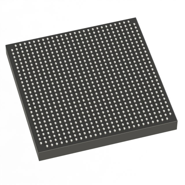
| Device Package | 780-FBGA (29x29) | Grade | Commercial | Operating Temperature | 0°C – 85°C | ||
|---|---|---|---|---|---|---|---|
| Package / Case | 780-BBGA, FCBGA | Number of I/O | 488 | Voltage | 860 mV - 1.15 V | ||
| Mounting Method | Surface Mount | RoHS Compliance | RoHS Compliant | REACH Compliance | REACH Unaffected | ||
| Moisture Sensitivity Level | 3 (168 Hours) | Number of LABs/CLBs | 4300 | Number of Logic Elements/Cells | 107500 | ||
| Number of Gates | N/A | ECCN | N/A | HTS Code | N/A | ||
| Qualification | N/A | Total RAM Bits | 4992000 |
Overview of EP3SL110F780C3G – Field Programmable Gate Array (FPGA) IC
The EP3SL110F780C3G is an Intel Stratix III family FPGA offering high-density programmable logic and on-chip memory for performance-oriented logic, DSP, and embedded designs. Built on the Stratix III architecture, it targets applications that require a combination of large logic capacity, significant embedded RAM, and flexible high-speed I/O support.
Key value propositions include a large logic fabric (approximately 107,500 logic elements), substantial embedded memory (approximately 4.99 Mbits), and family-level power and I/O capabilities such as selectable core voltage and programmable power management for balancing performance and power.
Key Features
- Logic Capacity Approximately 107,500 logic elements suitable for large FPGA designs and complex logic functions.
- Embedded Memory Approximately 4.99 Mbits of on-chip RAM to support data buffering, FIFOs, and local memory structures.
- I/O and Package 488 user I/O pins in a 780-pin FCBGA package (780-FBGA, 29×29); surface-mount mounting for compact board implementations.
- Power and Core Voltage Supports core voltage range from 0.86 V to 1.15 V; Stratix III family features such as Programmable Power Technology and selectable core voltage help tune performance versus power.
- DSP and Timing (Family Features) Stratix III family includes high-speed DSP blocks, multiple clock domains and PLL resources to support signal processing and timing-critical applications.
- High‑Speed I/O and Memory Interface Support (Family Features) Family-level support for SERDES and high-speed external memory interfaces enables integration with DDR-class memories and high-throughput links.
- Security and Reliability (Family Features) Optional 256-bit AES configuration-bitstream encryption and configuration memory error-detection features are available within the Stratix III family.
- Operating Range and Compliance Commercial grade operation from 0 °C to 85 °C; RoHS-compliant component.
Typical Applications
- High-Performance DSP Implement multi-channel signal processing, filtering, and compute-intensive algorithms using the device’s large logic and embedded memory resources.
- Communications and Networking Use the FPGA’s high-density I/O and family-level SERDES/memory-interface capabilities for packet processing, switching fabrics, and protocol bridging.
- Embedded Systems and Prototyping Rapidly prototype system-on-chip functions or replace custom logic with a programmable solution leveraging abundant logic elements and local RAM.
- Memory Interface and Controller Logic Implement controllers and interfaces for external DDR-class memories using the family’s dedicated memory interface support and DQS logic.
Unique Advantages
- High logic density: Approximately 107,500 logic elements enable large, complex digital designs without immediate need for multi-device partitioning.
- Substantial on-chip RAM: Approximately 4.99 Mbits of embedded memory reduces dependence on external RAM for buffering and local storage.
- Flexible power/performance trade-offs: Core voltage range (0.86 V–1.15 V) and Stratix III programmable power features allow tuning for performance or power savings.
- Robust I/O in a compact package: 488 user I/Os in a 780-FBGA (29×29) package supports dense board-level implementations while maintaining broad signal connectivity.
- Security and reliability options: Family-level AES encryption and configuration memory error detection provide options for protecting bitstreams and improving availability.
- Commercial readiness: RoHS-compliant and specified for 0 °C to 85 °C operation for mainstream commercial applications.
Why Choose EP3SL110F780C3G?
The EP3SL110F780C3G combines a high logic element count and multi-megabit embedded memory within the Stratix III family architecture, making it suitable for designers who need a programmable platform for intensive logic and memory-centric tasks. Its package and I/O density support compact, connectivity-rich board layouts while family-level features provide configurable power management and interface flexibility.
This device is well suited for engineering teams building DSP systems, communication endpoints, memory-interface controllers, or large-scale prototypes that benefit from a scalable FPGA family architecture and available security and reliability features.
Request a quote or submit a procurement inquiry for EP3SL110F780C3G to receive pricing and availability information through your preferred purchasing channel.


Date Founded: 1968
Headquarters: Santa Clara, California, USA
Employees: 130,000+
Revenue: $54.23 Billion
Certifications and Memberships: ISO9001:2015, ISO14001:2015, ISO17025:2017, ISO27001:2022, ISO45001:2018, ISO50001:2018


