
EP3SL110F780C4LG
| Part Description |
Field Programmable Gate Array (FPGA) IC |
|---|---|
| Quantity | 160 Available (as of October 8, 2026) |

| Product Category | Field Programmable Gate Array (FPGA) |
|---|---|
| Manufacturer | Intel |
| Manufacturing Status | Active |
| Manufacturer Standard Lead Time | 26 Weeks |
| Datasheet |
Specifications & Environmental
| Device Package | 780-FBGA (29x29) | Grade | Commercial | Operating Temperature | 0°C – 85°C | ||
|---|---|---|---|---|---|---|---|
| Package / Case | 780-BBGA, FCBGA | Number of I/O | 488 | Voltage | 860 mV - 1.15 V | ||
| Mounting Method | Surface Mount | RoHS Compliance | RoHS Compliant | REACH Compliance | REACH Unaffected | ||
| Moisture Sensitivity Level | 3 (168 Hours) | Number of LABs/CLBs | 4300 | Number of Logic Elements/Cells | 107500 | ||
| Number of Gates | N/A | ECCN | N/A | HTS Code | N/A | ||
| Qualification | N/A | Total RAM Bits | 4992000 |
Overview of EP3SL110F780C4LG – Field Programmable Gate Array (FPGA) IC
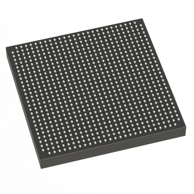
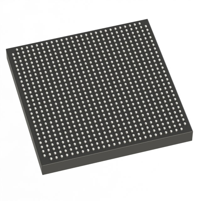
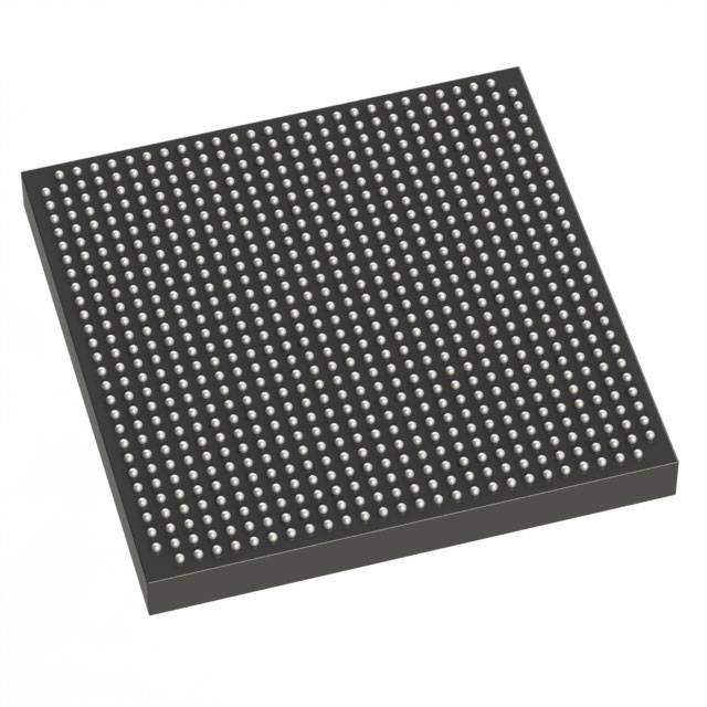
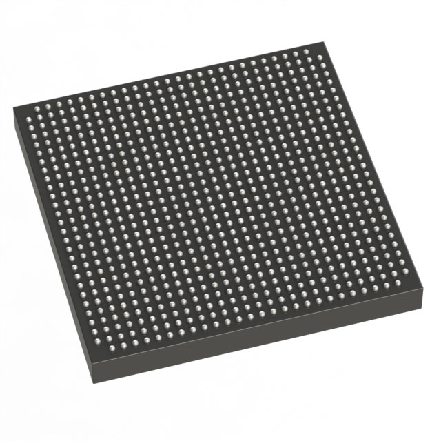
The EP3SL110F780C4LG is an Intel FPGA device supplied in a 780‑ball FCBGA package. It combines high logic capacity, multi-megabit on-chip memory, and extensive I/O to support demanding logic, DSP and embedded designs.
Leveraging features described in the Stratix III device family documentation, the device targets applications that require dense programmable logic, configurable power options, and system-level reliability features while operating over a commercial temperature range.
Key Features
- Logic Capacity Approximately 107,500 logic elements to implement complex digital designs and custom logic functions.
- Embedded Memory Approximately 4.99 Mbits of on-chip RAM for buffering, FIFOs and state storage in system designs.
- I/O Density 488 user I/O pins provided for broad external connectivity and modular I/O bank architectures referenced in the device family.
- High-Density Package 780-FBGA supplier device package (780‑BBGA / FCBGA) in the specified 780-ball format (29x29) for surface-mount integration.
- Core Voltage Range Selectable core supply range from 860 mV to 1.15 V to balance performance and power consumption.
- Commercial Temperature Grade Specified to operate from 0 °C to 85 °C for commercial applications.
- Power and Reliability Features (family) Programmable Power Technology and selectable core voltage are described in the Stratix III family handbook to optimize power vs. performance.
- Security and Error Detection (family) Stratix III family features include optional AES 256-bit configuration encryption and configuration memory CRC and ECC for enhanced design protection and reliability.
- Clocking and DSP Support (family) Family-level features include multiple global and regional clocks, PLLs, and high-speed DSP block support useful for signal processing and high-performance logic functions.
- RoHS Compliant Device is RoHS compliant for environmental compliance requirements.
Typical Applications
- High-Performance Logic and Control Implement complex state machines, protocol processing, and custom accelerators using the device’s dense logic element count.
- Digital Signal Processing On-chip memory and family DSP block features enable FIR filters, MAC arrays, and other real-time signal processing tasks.
- Memory Interface and Buffering Embedded RAM and configurable I/O banks support interface controllers, buffering and high-throughput data paths.
- Embedded Systems and Soft Processors Use the logic and memory resources for embedded control, offload functions or to host soft-core processors within application designs.
Unique Advantages
- High logic density: 107,500 logic elements provide the capacity for large-scale, programmable designs without external logic proliferation.
- Multi-megabit embedded memory: Approximately 4.99 Mbits of on-chip RAM reduces external memory needs for many buffering and stateful functions.
- Flexible power scaling: Selectable core voltage (860 mV–1.15 V) enables designers to tune performance versus power for system-level optimization.
- Robust system-level features: Family-documented options such as AES configuration encryption, CRC/ECC for configuration memory, and PLL/clocking resources support secure and reliable designs.
- Broad I/O availability: 488 user I/Os in a modular bank structure facilitate interfacing to multiple peripherals and memory devices.
- Surface-mount, high-density package: 780-ball FCBGA packaging supports compact board layouts while maintaining high I/O and signal integrity capabilities.
Why Choose EP3SL110F780C4LG?
EP3SL110F780C4LG is positioned for designers who need a high-capacity, commercially graded FPGA with multi-megabit embedded memory and extensive I/O in a compact surface-mount FCBGA package. The device’s selectable core voltage and family-documented power-management features allow designers to balance performance and power consumption for system needs.
Combined with family-level stability features—configuration encryption, error detection/correction, and plentiful clocking resources—this FPGA is suitable for applications requiring dense programmable logic, embedded processing, and reliable operation within the specified commercial temperature and supply ranges.
Request a quote or submit an inquiry to obtain pricing, availability, and lead-time details for EP3SL110F780C4LG.

























Date Founded: 1968
Headquarters: Santa Clara, California, USA
Employees: 130,000+
Revenue: $54.23 Billion
Certifications and Memberships: ISO9001:2015, ISO14001:2015, ISO17025:2017, ISO27001:2022, ISO45001:2018, ISO50001:2018


