
EP3SL110F780I4G
| Part Description |
Field Programmable Gate Array (FPGA) IC |
|---|---|
| Quantity | 1,401 Available (as of June 14, 2026) |

| Product Category | Field Programmable Gate Array (FPGA) |
|---|---|
| Manufacturer | Intel |
| Manufacturing Status | Active |
| Manufacturer Standard Lead Time | 26 Weeks |
| Datasheet |
Specifications & Environmental
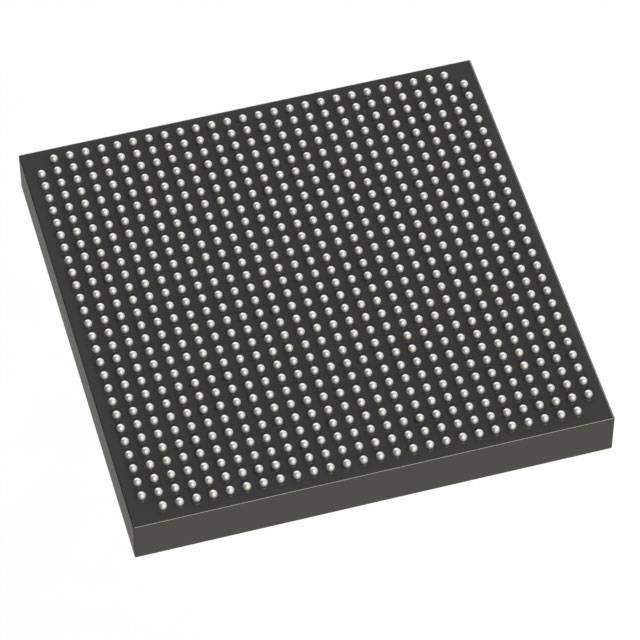
| Device Package | 780-FBGA (29x29) | Grade | Industrial | Operating Temperature | -40°C – 100°C | ||
|---|---|---|---|---|---|---|---|
| Package / Case | 780-BBGA, FCBGA | Number of I/O | 488 | Voltage | 860 mV - 1.15 V | ||
| Mounting Method | Surface Mount | RoHS Compliance | RoHS Compliant | REACH Compliance | REACH Unaffected | ||
| Moisture Sensitivity Level | 3 (168 Hours) | Number of LABs/CLBs | 4300 | Number of Logic Elements/Cells | 107500 | ||
| Number of Gates | N/A | ECCN | N/A | HTS Code | N/A | ||
| Qualification | N/A | Total RAM Bits | 4992000 |
Overview of EP3SL110F780I4G – Field Programmable Gate Array (FPGA) IC
The EP3SL110F780I4G is an Intel Stratix III family FPGA offered in a 780-ball FCBGA package. It provides a high-density FPGA fabric with approximately 107,500 logic elements, roughly 4.99 Mbits of embedded memory, and 488 user I/O pins suited for demanding embedded, signal-processing, and communications designs.
Built around Stratix III architecture features, this device targets high-performance logic, DSP, and memory-interface applications where configurable logic capacity, high-speed I/O, and industrial temperature operation are required. The device supports low-voltage core operation and on-chip features that address performance, power management, and configuration integrity.
Key Features
- Logic Capacity — Approximately 107,500 logic elements to implement complex custom logic and control functions.
- Embedded Memory — Approximately 4.99 Mbits of on-chip RAM for FIFOs, buffers, and local data storage.
- User I/O — 488 user I/O pins providing flexible interfacing to peripherals and external memories.
- Stratix III Architecture — Family-level features include high-speed DSP blocks (9×9, 12×12, 18×18, 36×36 multipliers), selectable core voltage, and Programmable Power Technology to balance performance and power.
- Clocking and Timing — Architecture-level support for multiple global, regional, and peripheral clocks and up to 12 PLLs for clock synthesis and dynamic phase control.
- High-speed I/O & Signal Integrity — Series-level features such as SERDES support, dynamic on-chip termination (OCT), and output delay/current-strength control for robust high-speed interfaces.
- Security & Reliability — Series-level support for 256-bit AES configuration-bitstream encryption and built-in CRC/ECC circuitry for configuration and memory error detection and correction.
- Power & Voltage — Device core supply range 860 mV–1.15 V with selectable core voltage options from the Stratix III family for power/performance tradeoffs.
- Package & Mounting — 780-ball FCBGA (780-FBGA, 29×29) surface-mount package for compact, system-level integration.
- Industrial Temperature Range — Rated for operation from −40 °C to 100 °C and RoHS compliant.
Typical Applications
- High-performance DSP systems — Implement demanding signal-processing pipelines using the device’s dedicated multiplier/DSP resources and abundant logic elements.
- Networking & Communications — Implement protocol processing, SERDES interfaces, and memory buffering for networking equipment and data-path subsystems.
- Memory Interface Controllers — Use on-chip memory and I/O to implement DDR/DDR2/DDR3 and other external memory interfaces supported by the Stratix III architecture.
- Embedded Systems & Custom Logic — Integrate custom control, preprocessing, and glue logic in compact FCBGA form for industrial embedded platforms.
Unique Advantages
- High Logic Density: Approximately 107,500 logic elements enable large-scale integration of custom logic and control functions, reducing external glue logic.
- Significant On-Chip Memory: Approximately 4.99 Mbits of embedded RAM supports large buffers, FIFOs, and local data storage for low-latency data paths.
- Flexible I/O Count: 488 user I/Os allow multiple parallel interfaces and broad connectivity options without additional multiplexing hardware.
- Industrial Temperature Rating: Specified −40 °C to 100 °C for deployment in industrial environments where extended temperature range is required.
- Configurable Power/Performance: Core voltage range (860 mV–1.15 V) and family-level Programmable Power Technology allow designers to tune performance versus power consumption.
- Robust System-level Features: Architecture-level support for AES encryption, CRC/ECC, PLLs, and advanced I/O features helps address security, reliability, and high-speed interface needs.
Why Choose EP3SL110F780I4G?
The EP3SL110F780I4G combines substantial logic and memory resources with a comprehensive set of Stratix III family features to support high-performance, reliable designs. Its 780-ball FCBGA packaging and industrial temperature rating make it suitable for space-constrained and environmentally demanding applications that require configurable, high-throughput hardware acceleration and flexible I/O.
Choose this device when your design requires a balance of large programmable logic capacity, on-chip memory, extensive I/O, and architecture-level capabilities such as advanced clocking, DSP support, and configuration security—all backed by Intel’s Stratix III device feature set.
Request a quote or submit an inquiry to get pricing and availability for EP3SL110F780I4G. Our team can provide lead-time and ordering information to support your project timeline.


Date Founded: 1968
Headquarters: Santa Clara, California, USA
Employees: 130,000+
Revenue: $54.23 Billion
Certifications and Memberships: ISO9001:2015, ISO14001:2015, ISO17025:2017, ISO27001:2022, ISO45001:2018, ISO50001:2018


