
EP3SL150F1152C2G
| Part Description |
Field Programmable Gate Array (FPGA) IC |
|---|---|
| Quantity | 281 Available (as of June 18, 2026) |

| Product Category | Field Programmable Gate Array (FPGA) |
|---|---|
| Manufacturer | Intel |
| Manufacturing Status | Active |
| Manufacturer Standard Lead Time | 26 Weeks |
| Datasheet |
Specifications & Environmental
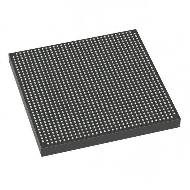
| Device Package | 1152-FBGA (35x35) | Grade | Commercial | Operating Temperature | 0°C – 85°C | ||
|---|---|---|---|---|---|---|---|
| Package / Case | 1152-BBGA, FCBGA | Number of I/O | 744 | Voltage | 860 mV - 1.15 V | ||
| Mounting Method | Surface Mount | RoHS Compliance | RoHS Compliant | REACH Compliance | REACH Unaffected | ||
| Moisture Sensitivity Level | 3 (168 Hours) | Number of LABs/CLBs | 5700 | Number of Logic Elements/Cells | 142500 | ||
| Number of Gates | N/A | ECCN | N/A | HTS Code | N/A | ||
| Qualification | N/A | Total RAM Bits | 6543360 |
Overview of EP3SL150F1152C2G – Field Programmable Gate Array (FPGA) IC
The EP3SL150F1152C2G is a high-density FPGA from Intel, built on the Stratix III device family architecture. It delivers a large logic fabric and embedded memory density suitable for high-performance logic, DSP, and embedded system designs where integration and I/O capacity matter.
Targeted at commercial applications, this surface-mount FCBGA device combines approximately 142,500 logic elements with approximately 6.54 Mbits of embedded memory and 744 user I/O pins, enabling complex combinational and sequential logic, memory buffering, and rich I/O interfacing in a single package.
Key Features
- Logic Capacity Approximately 142,500 logic elements for large-scale logic integration and complex design implementation.
- Embedded Memory Approximately 6.54 Mbits of on-chip memory to support FIFOs, buffering, and local data storage without external RAM.
- I/O and Banked Architecture 744 user I/O pins in a high-pin-count FBGA package, enabling broad peripheral connectivity and parallel interfaces.
- High-pin-count Package 1152-FBGA (35×35) package case (1152-BBGA/FCBGA), surface-mount mounting for dense board-level integration.
- Core Voltage Range Core supply range from 0.860 V to 1.15 V to match system power requirements and performance targets.
- Commercial Temperature Grade Operating temperature range of 0 °C to 85 °C for standard commercial environments.
- Stratix III Family Capabilities Family-level features include DSP blocks for multiply-accumulate tasks, up to 12 PLLs, multi-clock support, dynamic on-chip termination, and optional 256-bit AES configuration security.
- Standards & Compliance RoHS-compliant device suitable for environmentally regulated designs.
Typical Applications
- High-performance signal processing Implement FIR filters, DSP pipelines, and custom arithmetic using the device's logic density and embedded memory.
- Networking and communications Build protocol engines, packet processing, and interface bridging that leverage abundant I/O and family support for high-speed serial and parallel interfaces.
- Memory interface controllers Implement custom controllers and buffering for external memory interfaces using on-chip RAM and flexible I/O.
- Embedded system integration Integrate peripherals, custom accelerators, and soft processors for system-on-chip style designs in a single FPGA package.
Unique Advantages
- High integration density: Approximately 142,500 logic elements and 6.54 Mbits of embedded memory reduce the need for external components and simplify board-level BOM.
- Extensive I/O capability: 744 user I/O pins in a 1152-FBGA footprint provide ample connectivity for parallel buses, peripherals, and mixed-signal interfaces.
- Configurable power points: Core supply range of 0.860–1.15 V supports power/performance trade-offs and integration into diverse system power architectures.
- Commercial-grade reliability: Rated for 0 °C to 85 °C operation and RoHS compliant for mainstream commercial deployments.
- Stratix III family feature set: Access to family-level capabilities such as DSP blocks, PLLs, clocking resources, dynamic on-chip termination, and optional AES configuration security to accelerate system design.
- Surface-mount FBGA packaging: 1152-FBGA (35×35) package enables compact, high-pin-count board layouts for space-constrained systems.
Why Choose EP3SL150F1152C2G?
The EP3SL150F1152C2G is positioned for designers who require substantial logic resources, meaningful on-chip memory, and broad I/O in a commercial-grade FPGA. Its combination of approximately 142,500 logic elements, roughly 6.54 Mbits of embedded RAM, and 744 user I/Os provides a balanced platform for compute- and I/O-intensive designs.
Backed by the Stratix III family capabilities highlighted in the device handbook, this FPGA is suitable for engineers implementing high-performance DSP, protocol processing, custom memory interfaces, and integrated embedded systems where long-term scalability and a mature device feature set are important.
Request a quote or submit a product inquiry for EP3SL150F1152C2G to receive pricing and availability details tailored to your design and volume needs.


Date Founded: 1968
Headquarters: Santa Clara, California, USA
Employees: 130,000+
Revenue: $54.23 Billion
Certifications and Memberships: ISO9001:2015, ISO14001:2015, ISO17025:2017, ISO27001:2022, ISO45001:2018, ISO50001:2018


