
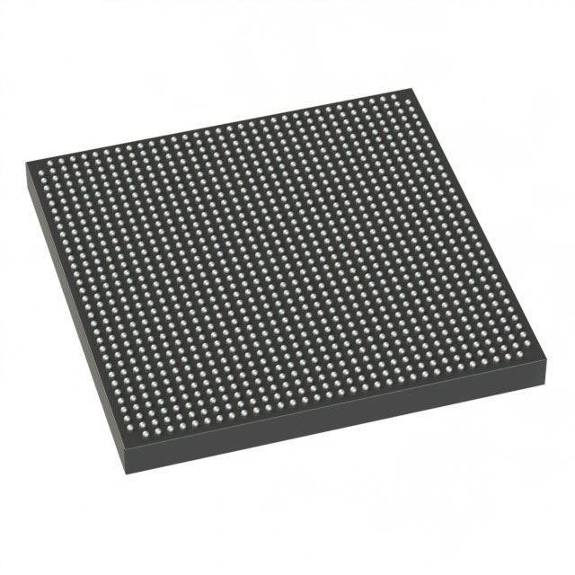
EP3SL150F1152C2N
| Part Description |
Stratix® III L Field Programmable Gate Array (FPGA) IC 744 6543360 142500 1152-BBGA, FCBGA |
|---|---|
| Quantity | 684 Available (as of June 15, 2026) |

| Product Category | Field Programmable Gate Array (FPGA) |
|---|---|
| Manufacturer | Intel |
| Manufacturing Status | Obsolete |
| Manufacturer Standard Lead Time | Contact Us |
| Datasheet |
Specifications & Environmental
| Device Package | 1152-FBGA (35x35) | Grade | Commercial | Operating Temperature | 0°C – 85°C | ||
|---|---|---|---|---|---|---|---|
| Package / Case | 1152-BBGA, FCBGA | Number of I/O | 744 | Voltage | 860 mV - 1.15 V | ||
| Mounting Method | Surface Mount | RoHS Compliance | RoHS Compliant | REACH Compliance | REACH Unknown | ||
| Moisture Sensitivity Level | 4 (72 Hours) | Number of LABs/CLBs | 5700 | Number of Logic Elements/Cells | 142500 | ||
| Number of Gates | N/A | ECCN | 3A001A7A | HTS Code | 8542.31.0001 | ||
| Qualification | N/A | Total RAM Bits | 6543360 |
Overview of EP3SL150F1152C2N – Stratix® III L FPGA, 142,500 Logic Elements
The EP3SL150F1152C2N is a Stratix® III L Field Programmable Gate Array (FPGA) IC from Intel, packaged in a 1152-ball FCBGA (1152-FBGA, 35×35) surface-mount package. It combines a large logic array with substantial on-chip memory and a high I/O count to support complex, high-density digital designs.
Targeted for applications that require extensive fabric resources, embedded memory, and dense I/O, this device is suitable for systems integrating external memory interfaces, DSP functions, and high-speed I/O fabrics within a commercial temperature range.
Key Features
- Logic Capacity Approximately 142,500 logic elements providing a large programmable fabric for complex logic, control and datapath implementations.
- Logic Array Blocks 5,700 logic array blocks (LABs) to structure logic resources for efficient synthesis and placement.
- Embedded Memory Approximately 6.54 Mbits of on-chip RAM (6,543,360 total RAM bits) for buffering, FIFOs, and on-chip data storage.
- High I/O Density 744 I/O pins to support multiple external interfaces and parallel connections to memory and peripherals.
- Power Supply Nominal core voltage range from 0.860 V to 1.15 V for core power planning and supply design.
- Package & Mounting 1152-BBGA (FCBGA) surface-mount package in a 35×35 ball format for high-density board-level integration.
- Operating Temperature & Grade Commercial grade operation from 0 °C to 85 °C for standard temperature-range applications.
- Compliance RoHS compliant to support lead-free manufacturing processes.
- Documented Architecture Supported by Stratix III device handbook material covering architecture, memory blocks, DSP blocks, clocking, I/O structure, and configuration.
Typical Applications
- High‑Performance Signal Processing On-chip DSP blocks and large logic and memory resources make the device suitable for implementing complex signal-processing pipelines.
- Communications & Networking High I/O count and support for external memory interfaces enable packet-processing, line-rate buffering, and protocol bridging.
- Memory Interface Controllers Resources and documented external memory interface support facilitate custom memory controller and interface designs.
- Prototyping and System Integration Dense logic fabric and extensive I/O enable system prototypes that require integration of multiple peripherals and subsystems on a single FPGA.
Unique Advantages
- Large programmable fabric: 142,500 logic elements provide headroom for complex designs and parallel datapaths.
- Substantial embedded memory: Approximately 6.54 Mbits of on-chip RAM reduces dependency on external memory for many buffering and storage needs.
- High I/O count: 744 I/Os support multiple external interfaces and wide parallel buses without external multiplexing.
- Compact, high-density package: 1152-ball FCBGA (35×35) enables a small board footprint for high-functionality systems.
- Commercial temperature rating: 0 °C to 85 °C operation aligns with standard commercial deployments and system-level thermal plans.
- Standards-based documentation: Stratix III device handbook material provides architecture, configuration, and design guidance to support development and integration.
Why Choose EP3SL150F1152C2N?
The EP3SL150F1152C2N delivers a combination of large logic capacity, substantial embedded memory, and high I/O density in a compact FCBGA package, making it well suited for advanced digital designs that demand significant on-chip resources. Its documented Stratix III architecture elements—memory blocks, DSP blocks, I/O structure, and configuration features—help engineers map complex algorithms and interface requirements into a single programmable device.
This device is ideal for teams building high-density, performance‑oriented systems in commercial environments who need a programmable solution with extensive resources, robust documentation, and RoHS compliance for lead‑free manufacturing workflows.
Request a quote or submit a procurement inquiry to get pricing and availability for the EP3SL150F1152C2N. Our team can provide technical support and ordering assistance to help integrate this Stratix III L FPGA into your next design.


Date Founded: 1968
Headquarters: Santa Clara, California, USA
Employees: 130,000+
Revenue: $54.23 Billion
Certifications and Memberships: ISO9001:2015, ISO14001:2015, ISO17025:2017, ISO27001:2022, ISO45001:2018, ISO50001:2018


