
EP3SL150F780C2G
| Part Description |
Field Programmable Gate Array (FPGA) IC |
|---|---|
| Quantity | 817 Available (as of October 8, 2026) |

| Product Category | Field Programmable Gate Array (FPGA) |
|---|---|
| Manufacturer | Intel |
| Manufacturing Status | Active |
| Manufacturer Standard Lead Time | 26 Weeks |
| Datasheet |
Specifications & Environmental
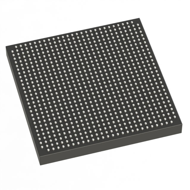
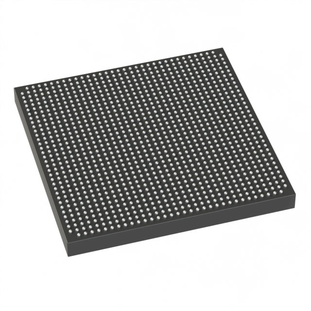
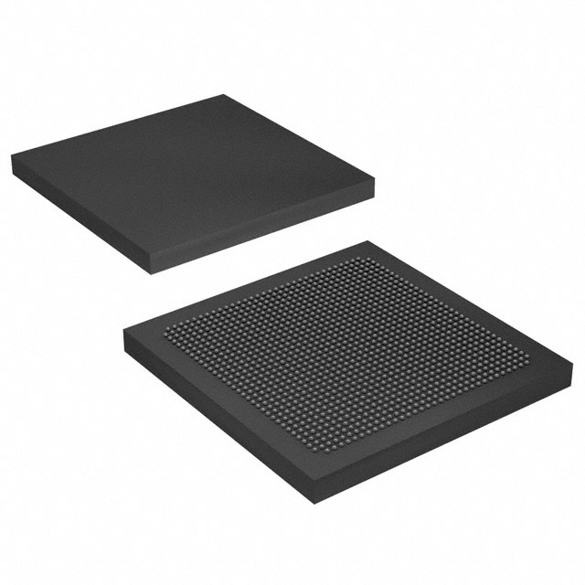
| Device Package | 780-FBGA (29x29) | Grade | Commercial | Operating Temperature | 0°C – 85°C | ||
|---|---|---|---|---|---|---|---|
| Package / Case | 780-BBGA, FCBGA | Number of I/O | 488 | Voltage | 860 mV - 1.15 V | ||
| Mounting Method | Surface Mount | RoHS Compliance | RoHS Compliant | REACH Compliance | REACH Unaffected | ||
| Moisture Sensitivity Level | 3 (168 Hours) | Number of LABs/CLBs | 5700 | Number of Logic Elements/Cells | 142500 | ||
| Number of Gates | N/A | ECCN | N/A | HTS Code | N/A | ||
| Qualification | N/A | Total RAM Bits | 6543360 |
Overview of EP3SL150F780C2G – Field Programmable Gate Array (FPGA) IC
The EP3SL150F780C2G is an Intel Stratix III family field programmable gate array optimized for high-performance logic, digital signal processing and embedded system integration. It combines a high logic-element count and multi-megabit embedded memory with low-voltage core operation and a compact surface-mount FCBGA package for dense system designs.
Targeted at commercial applications, this device delivers configurable performance and power control alongside a broad I/O complement and on-chip features intended for high-speed connectivity, memory interfacing and DSP workloads.
Key Features
- Logic Capacity — 142,500 logic elements to implement complex combinational and sequential logic functions.
- Embedded Memory — Approximately 6.54 Mbits of on-chip RAM for FIFOs, buffers and storage-intensive functions.
- I/O and Packaging — 488 user I/O pins in a 780-FBGA (29×29) surface-mount FCBGA package, suitable for compact, board-level integration.
- Core Voltage Range — Configurable core supply between 0.860 V and 1.15 V to enable selectable performance vs. power operation.
- Operating Range and Grade — Commercial-grade device rated for 0 °C to 85 °C operating temperature and RoHS-compliant.
- Programmable Power Technology — Family-level capability to reduce power by enabling and disabling blocks as required (as described in the Stratix III family documentation).
- DSP and Arithmetic Support — Stratix III family DSP resources including dedicated multiplier implementations and multiply-accumulate functions for signal processing workloads (family-level feature).
- Clocking and PLLs — Family-level support for extensive clocking resources including multiple global/regional/peripheral clocks and on-chip PLL reconfiguration.
- Security and Reliability — Family-level support for 256-bit AES configuration encryption and built-in error detection/correction mechanisms for configuration and memory integrity.
Typical Applications
- High-Performance DSP — Implement FIR filters, multiply-accumulate pipelines and custom signal-processing blocks using the device’s dedicated DSP resources and abundant logic elements.
- Memory Interface Controllers — Use embedded memory and modular I/O banks to build DDR/DDR2/DDR3 and other external memory interfaces.
- Networking & Communications — Deploy SERDES and high-speed I/O features (family-level) for protocol bridging, packet processing and custom networking functions.
- Embedded Systems & Acceleration — Integrate hardware accelerators, custom processors and control logic leveraging the device’s logic density and on-chip memory.
Unique Advantages
- High Logic Density: 142,500 logic elements provide the capacity to implement large-scale custom logic and complex state machines without external ASICs.
- Multi‑Mbit On‑Chip RAM: Approximately 6.54 Mbits of embedded memory reduces external memory bandwidth needs and simplifies board-level design.
- Configurable Power/Performance: Core voltage range (0.860–1.15 V) and family-level programmable power features allow designers to optimize for power or peak performance.
- Broad I/O in Compact Package: 488 I/O in a 780-FBGA (29×29) surface-mount package enables high pin-count designs in space-constrained applications.
- Security and Robustness: Family-level AES configuration encryption and error detection/correction features enhance IP protection and runtime reliability.
- Vendor Ecosystem Support: Stratix III family support for embedded processors and megafunction IP (as documented for the family) helps accelerate system integration and reduce development time.
Why Choose EP3SL150F780C2G?
The EP3SL150F780C2G combines substantial logic resources and multi-megabit embedded memory with configurable core-voltage operation and a dense 780-FBGA package to address demanding DSP, memory-interface and high-speed logic designs at commercial temperature ranges. Its family-level features for programmable power, security and extensive clocking/PLLs offer design flexibility for performance- and power-sensitive applications.
This device is well suited for engineering teams who need a scalable, programmable silicon platform with on-chip RAM, a large I/O count and the ecosystem support described in Intel’s Stratix III documentation to accelerate time-to-market and manage system-level integration.
Request a quote or submit an inquiry to receive pricing and availability for EP3SL150F780C2G and to discuss how this FPGA can fit your next design.

























Date Founded: 1968
Headquarters: Santa Clara, California, USA
Employees: 130,000+
Revenue: $54.23 Billion
Certifications and Memberships: ISO9001:2015, ISO14001:2015, ISO17025:2017, ISO27001:2022, ISO45001:2018, ISO50001:2018


