
EP3SL200F1152C2N
| Part Description |
Stratix® III L Field Programmable Gate Array (FPGA) IC 744 10901504 200000 1152-BBGA, FCBGA |
|---|---|
| Quantity | 237 Available (as of June 14, 2026) |

| Product Category | Field Programmable Gate Array (FPGA) |
|---|---|
| Manufacturer | Intel |
| Manufacturing Status | Obsolete |
| Manufacturer Standard Lead Time | Contact Us |
| Datasheet |
Specifications & Environmental
| Device Package | 1152-FBGA (35x35) | Grade | Commercial | Operating Temperature | 0°C – 85°C | ||
|---|---|---|---|---|---|---|---|
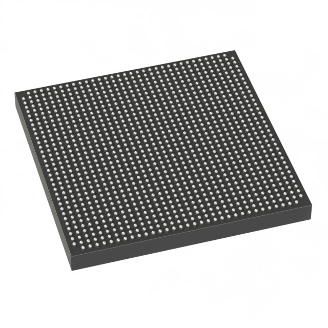
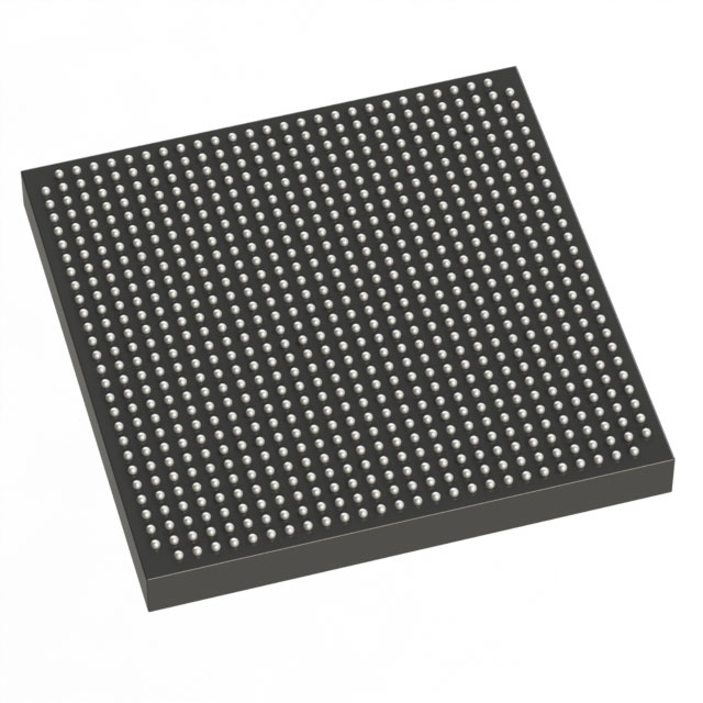
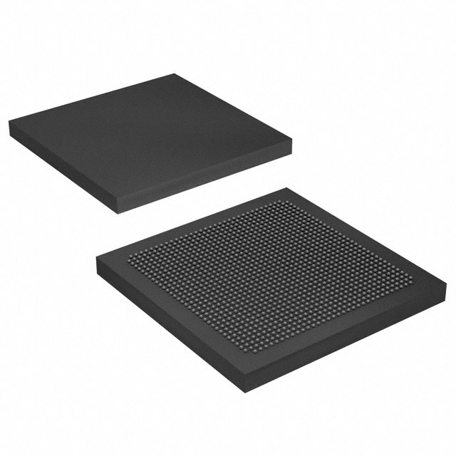
| Package / Case | 1152-BBGA, FCBGA | Number of I/O | 744 | Voltage | 860 mV - 1.15 V | ||
| Mounting Method | Surface Mount | RoHS Compliance | RoHS Compliant | REACH Compliance | REACH Unknown | ||
| Moisture Sensitivity Level | 3 (168 Hours) | Number of LABs/CLBs | 8000 | Number of Logic Elements/Cells | 200000 | ||
| Number of Gates | N/A | ECCN | 3A001A2C | HTS Code | 8542.39.0001 | ||
| Qualification | N/A | Total RAM Bits | 10901504 |
Overview of EP3SL200F1152C2N – Stratix® III L Field Programmable Gate Array (FPGA) IC 744 10901504 200000 1152-BBGA, FCBGA
The EP3SL200F1152C2N is a Stratix® III L field programmable gate array (FPGA) in a high-density 1152-ball FCBGA package. It provides a large number of logic elements, substantial embedded RAM, and a high I/O count for designs that require reconfigurable logic and on-chip memory.
Key device attributes include 200,000 logic elements, approximately 10.9 Mbits of total on-chip RAM, 744 I/O pins, low-voltage supply operation, and a commercial operating temperature range of 0 °C to 85 °C.
Key Features
- Core Logic Capacity Provides 200,000 logic elements to implement complex, high-density digital logic and state machines.
- Embedded Memory Approximately 10.9 Mbits of on-chip RAM to support buffering, lookup tables, and local data storage without external memory.
- I/O Density 744 available I/O pins to support multiple parallel interfaces, wide buses, and extensive peripheral connectivity.
- Package 1152-ball BGA/FCBGA package (1152-FBGA, 35×35) for compact board-level integration and high pin count in a surface-mount form factor.
- Power Supports a voltage supply range of 860 mV to 1.15 V to match system power domains and logic core requirements.
- Operating Range & Grade Commercial temperature rating from 0 °C to 85 °C; surface-mount mounting type for standard PCB assembly processes.
- Compliance RoHS compliant to meet common environmental requirements for lead-free assembly.
Typical Applications
- High-density digital processing: Use the device's 200,000 logic elements and ~10.9 Mbits of embedded memory to implement complex datapath and control logic for compute- and processing-intensive tasks.
- I/O-intensive interface hubs: Leverage 744 I/O pins to aggregate and bridge multiple parallel or serial interfaces on a single FPGA.
- Custom accelerators: Deploy as an on-board hardware accelerator where large logic capacity and embedded RAM reduce reliance on external processors and memory.
- Embedded system integration: Integrate control, glue logic, and buffering directly on the FPGA to minimize board-level component count and simplify system architecture.
Unique Advantages
- High logic density: 200,000 logic elements enable implementation of large, consolidated designs that would otherwise require multiple devices.
- Substantial on-chip memory: Approximately 10.9 Mbits of embedded RAM supports internal buffering and data staging without external RAM.
- Extensive I/O capability: 744 I/O pins provide flexibility for broad connectivity requirements and parallel signal routing.
- Compact, high-pin-count package: The 1152-ball FCBGA package offers a space-efficient solution for high-density boards while maintaining a large I/O complement.
- Low-voltage core operation: Core supply range of 860 mV to 1.15 V allows integration with modern low-voltage system domains.
- RoHS compliant: Meets lead-free assembly requirements for contemporary manufacturing environments.
Why Choose EP3SL200F1152C2N?
The EP3SL200F1152C2N positions itself as a high-capacity, memory-rich Stratix® III L FPGA suitable for designs that require significant programmable logic, on-chip RAM, and a large number of I/O signals in a compact surface-mount package. Its combination of 200,000 logic elements, approximately 10.9 Mbits of embedded memory, and 744 I/Os makes it appropriate for consolidating complex functions and reducing board-level component count within a commercial temperature range.
Designed for engineers who need substantial integration and configurability, this device supports scalable designs where logic density, embedded memory, and I/O capacity are primary drivers. Its RoHS compliance and standard FCBGA package simplify manufacturing and deployment across a range of commercial applications.
Request a quote or submit a procurement inquiry to obtain pricing and availability for EP3SL200F1152C2N.


Date Founded: 1968
Headquarters: Santa Clara, California, USA
Employees: 130,000+
Revenue: $54.23 Billion
Certifications and Memberships: ISO9001:2015, ISO14001:2015, ISO17025:2017, ISO27001:2022, ISO45001:2018, ISO50001:2018


