
EP3SL200F1152C2G
| Part Description |
Field Programmable Gate Array (FPGA) IC |
|---|---|
| Quantity | 1,964 Available (as of June 10, 2026) |
| Product Category | Field Programmable Gate Array (FPGA) |
|---|---|
| Manufacturer | Intel |
| Manufacturing Status | Active |
| Manufacturer Standard Lead Time | 26 Weeks |
| Datasheet |
Specifications & Environmental
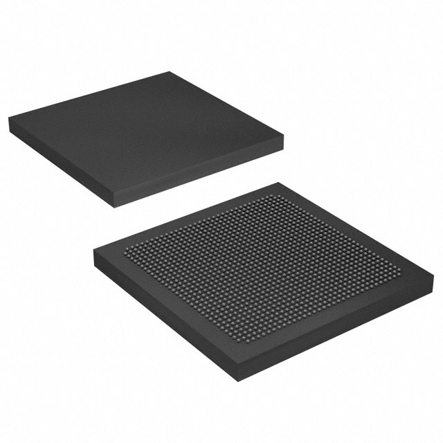
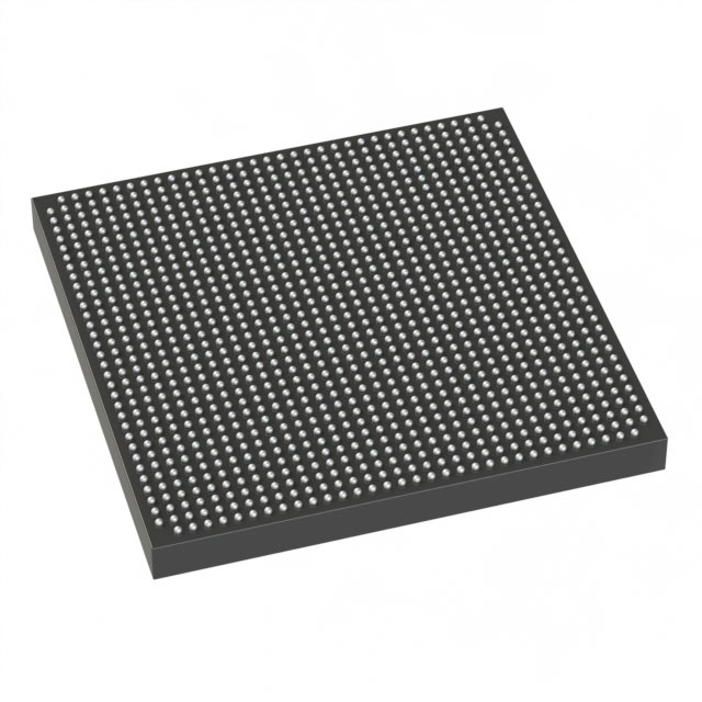
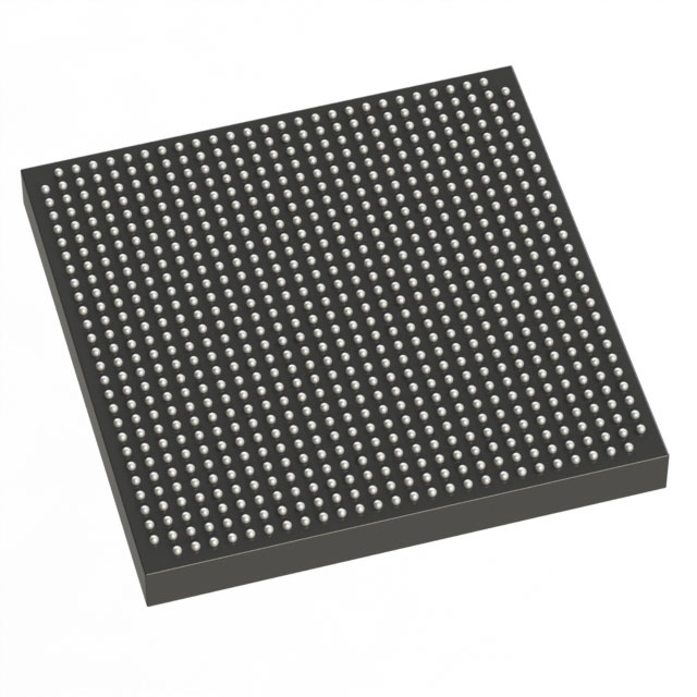
| Device Package | 1152-FBGA (35x35) | Grade | Commercial | Operating Temperature | 0°C – 85°C | ||
|---|---|---|---|---|---|---|---|
| Package / Case | 1152-BBGA, FCBGA | Number of I/O | 744 | Voltage | 860 mV - 1.15 V | ||
| Mounting Method | Surface Mount | RoHS Compliance | RoHS Compliant | REACH Compliance | REACH Unaffected | ||
| Moisture Sensitivity Level | 3 (168 Hours) | Number of LABs/CLBs | 8000 | Number of Logic Elements/Cells | 200000 | ||
| Number of Gates | N/A | ECCN | N/A | HTS Code | N/A | ||
| Qualification | N/A | Total RAM Bits | 10901504 |
Overview of EP3SL200F1152C2G – Field Programmable Gate Array (FPGA) IC
The EP3SL200F1152C2G is a Stratix III family FPGA optimized for high-performance logic, DSP and embedded applications. Built on the Stratix III architecture, it delivers a balance of high logic density, substantial on-chip memory and advanced I/O capabilities for data-path and system-level integration.
Key use cases include high-performance signal processing, complex interface bridging and programmable hardware acceleration in commercial applications. The device combines approximately 200,000 logic elements with roughly 10.9 Mbits of embedded memory, extensive I/O and selectable core-voltage operation to address demanding design requirements.
Key Features
- Stratix III architecture — Implements the Stratix III family feature set including Programmable Power Technology and selectable core voltage for optimized performance versus power tradeoffs.
- Logic capacity — Approximately 200,000 logic elements suitable for large-scale logic and control implementations.
- Embedded memory — Approximately 10.9 Mbits of on-chip RAM for large buffer and state-storage requirements.
- High-performance DSP support — Family-level support for dedicated DSP blocks and multipliers to accelerate signal-processing and arithmetic-intensive functions.
- Flexible clocking and PLLs — Stratix III family clocking resources including multiple global, regional and peripheral clocks plus up to 12 PLLs for clock synthesis and deskew.
- Robust I/O — 744 user I/O pins and modular I/O bank architecture with high-speed differential I/O and SERDES support for demanding interface requirements.
- Security and reliability — Family features include optional 256-bit AES encryption for configuration security, CRC for configuration memory checking and ECC for on-chip memory protection.
- Package and mounting — 1152-FBGA (35×35) surface-mount FCBGA package for high-density board integration.
- Power and operating range — Core supply range from 860 mV to 1.15 V and commercial operating temperature from 0 °C to 85 °C.
- RoHS compliant — Supplied in a lead-free, RoHS-compliant package.
Typical Applications
- High-performance signal processing — Implement FIR filters, FFTs and other DSP algorithms using the device’s high logic count and dedicated multiplier resources.
- Network and communications interfaces — Use the modular I/O banks, SERDES and timing resources to implement high-speed links and protocol bridging.
- Memory interface controllers — Deploy the on-chip memory and I/O capabilities for DDR/DDR2/DDR3 and other external memory interfaces in packet buffering and data staging roles.
- Hardware acceleration — Offload compute-intensive tasks from CPUs by implementing custom accelerators and coprocessors in programmable logic.
Unique Advantages
- Substantial logic and memory in one device: Combines approximately 200,000 logic elements with ~10.9 Mbits of embedded RAM to reduce external memory and component count.
- Flexible power-performance trade-offs: Selectable core voltage and Programmable Power Technology enable designers to tune the device for required performance or lower power consumption.
- Comprehensive system-level features: Integrated clocking, PLLs, SERDES and modular I/O simplify complex interface and timing designs.
- Security and data integrity: Built-in AES configuration encryption, CRC and ECC support protect designs and improve runtime reliability.
- High-density package: 1152-FBGA (35×35) package supports dense pinout and high I/O counts while enabling surface-mount assembly.
Why Choose EP3SL200F1152C2G?
The EP3SL200F1152C2G positions itself as a high-capacity, system-oriented FPGA offering the Stratix III family’s balance of logic density, embedded memory and I/O flexibility. It is suited for commercial designs that require sizable programmable logic, robust DSP capability and secure configuration options within a surface-mount FBGA package.
Designers benefit from an established family feature set—extensive clocking, PLLs, SERDES support and on-chip memory protection—helping accelerate time-to-market while maintaining scalability and long-term support within the Stratix III ecosystem.
Request a quote or submit an inquiry to obtain pricing, lead times and ordering information for EP3SL200F1152C2G.


Date Founded: 1968
Headquarters: Santa Clara, California, USA
Employees: 130,000+
Revenue: $54.23 Billion
Certifications and Memberships: ISO9001:2015, ISO14001:2015, ISO17025:2017, ISO27001:2022, ISO45001:2018, ISO50001:2018


