
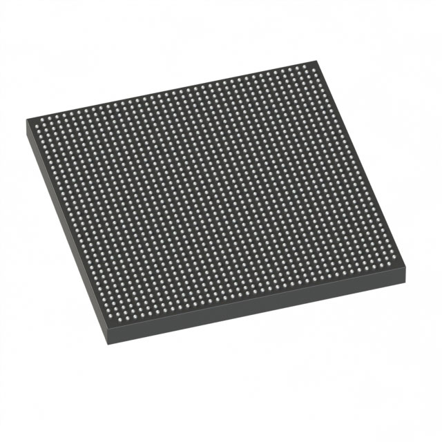
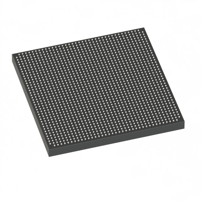
EP3SL340F1517C3NAA
| Part Description |
Stratix® III L Field Programmable Gate Array (FPGA) IC 976 18822144 337500 1517-BBGA, FCBGA |
|---|---|
| Quantity | 279 Available (as of October 7, 2026) |
| Product Category | Field Programmable Gate Array (FPGA) |
|---|---|
| Manufacturer | Intel |
| Manufacturing Status | Obsolete |
| Manufacturer Standard Lead Time | Contact Us |
| Datasheet |
Specifications & Environmental
| Device Package | 1517-FBGA (40x40) | Grade | Commercial | Operating Temperature | 0°C – 85°C | ||
|---|---|---|---|---|---|---|---|
| Package / Case | 1517-BBGA, FCBGA | Number of I/O | 976 | Voltage | 860 mV - 1.15 V | ||
| Mounting Method | Surface Mount | RoHS Compliance | RoHS non-compliant | REACH Compliance | REACH Unknown | ||
| Moisture Sensitivity Level | 4 (72 Hours) | Number of LABs/CLBs | 135000 | Number of Logic Elements/Cells | 337500 | ||
| Number of Gates | N/A | ECCN | OBSOLETE | HTS Code | N/A | ||
| Qualification | N/A | Total RAM Bits | 18822144 |
Overview of EP3SL340F1517C3NAA – Stratix® III L FPGA, 1517‑BBGA
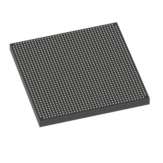
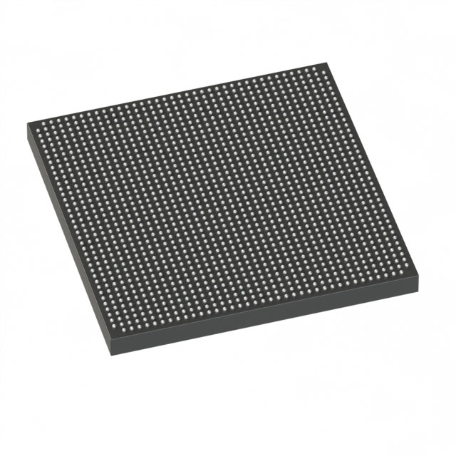
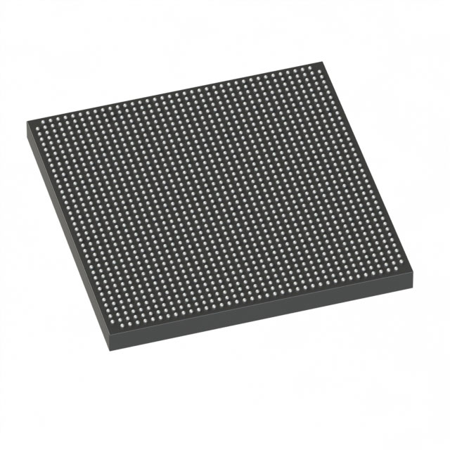
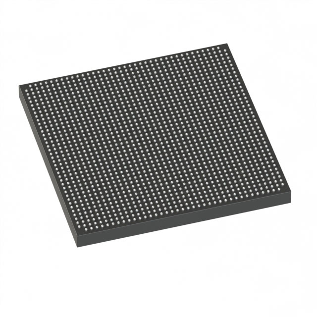
The EP3SL340F1517C3NAA is a Stratix® III L field programmable gate array (FPGA) in a 1517‑BBGA (40×40) FCBGA surface‑mount package. Designed for high‑performance logic, DSP and embedded applications, this device combines a large logic fabric with substantial on‑chip memory and a broad I/O complement to support complex system integration.
Built on the Stratix III device architecture, the device offers programmable power features and selectable core voltage to balance performance and power consumption, making it suitable for demanding designs in communications, signal processing, and high‑bandwidth interfacing within commercial temperature ranges.
Key Features
- Logic Capacity — 337,500 logic elements to implement complex state machines, datapaths and control logic.
- Embedded Memory — Approximately 18.8 Mbits of on‑chip RAM for large buffers, FIFOs and memory‑mapped structures.
- High I/O Density — 976 user I/O pins arranged for flexible bank configuration and external interfacing.
- Programmable Power and Core Voltage — Programmable Power Technology and selectable core voltage (0.86 V to 1.15 V) to tune power versus performance.
- DSP and Multiplier Support — Dedicated DSP resources with support for multipliers including 9×9, 12×12, 18×18 and 36×36 implementations as documented for the Stratix III family.
- Clocking and PLLs — Multi‑level clocking resources including global, regional and peripheral clocks, plus up to 12 phase‑locked loops for clock synthesis and dynamic phase control.
- High‑Speed I/O and SERDES — Differential I/O with SERDES and dynamic phase alignment circuitry supporting high‑speed serial interfaces (family‑level performance specified up to 1.6 Gbps).
- Memory Interface Support — Family support for common external memory interfaces (DDR, DDR2, DDR3, RLDRAM II, QDR II and QDR II+) and dedicated DQS logic on I/O banks.
- Signal Integrity Features — Dynamic on‑chip termination (OCT), output delay and programmable drive strength for improved signal integrity across I/O banks.
- Package and Mounting — 1517‑BBGA (FCBGA) supplier device package 1517‑FBGA (40×40); surface mount construction.
- Commercial Temperature Range — Rated for 0 °C to 85 °C operation and RoHS compliant.
Typical Applications
- High‑Performance DSP Systems — Leverage the device’s dedicated multipliers and large logic and memory resources for real‑time signal processing, filtering and FFT implementations.
- Networking & Communications — Use the high I/O count, SERDES capabilities and memory interface support to implement packet processing, protocol bridging and high‑speed link endpoints.
- Memory Interface Controllers — Implement controllers for DDR/DDR2/DDR3 and high‑performance SRAM interfaces using dedicated DQS logic and I/O bank features.
- Embedded Processing & Custom SoC — Integrate soft processors (e.g., Nios® II support noted for the family) with peripherals and custom accelerators on a single device.
Unique Advantages
- Highly integrated platform: Large logic capacity, abundant embedded memory and extensive I/O reduce external component count and simplify system design.
- Configurable power/performance tradeoffs: Selectable core voltage and programmable power features let designers optimize for throughput or energy efficiency.
- Robust DSP capability: Built‑in multiplier blocks and DSP resources accelerate math‑intensive kernels and signal chains without consuming general logic.
- Flexible clocking and timing: Multiple clock domains and up to 12 PLLs enable complex timing architectures and dynamic clock management.
- Signal integrity controls: Dynamic OCT, output delay and drive strength control help meet high‑speed interface timing and signal integrity requirements.
- Commercial‑grade, RoHS compliant: Designed for commercial temperature operation with RoHS compliance for global assembly requirements.
Why Choose EP3SL340F1517C3NAA?
The EP3SL340F1517C3NAA delivers a balance of high logic density, substantial embedded memory and a wide complement of I/O and clocking resources derived from the Stratix III L family. It is positioned for designs that require intensive DSP, complex interfacing and embedded processing within a commercial temperature envelope.
With programmable power options, selectable core voltage and family support for common memory interfaces and embedded processors, this device provides a scalable, technically capable foundation for system‑level integration and long‑term design flexibility backed by Stratix III documentation and IP support.
Request a quote or submit an inquiry to receive pricing and availability for the EP3SL340F1517C3NAA. Our team can assist with lead time and volume options to support your design and procurement needs.





















Date Founded: 1968
Headquarters: Santa Clara, California, USA
Employees: 130,000+
Revenue: $54.23 Billion
Certifications and Memberships: ISO9001:2015, ISO14001:2015, ISO17025:2017, ISO27001:2022, ISO45001:2018, ISO50001:2018


