
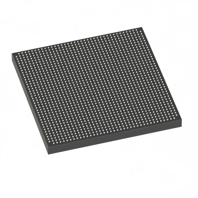
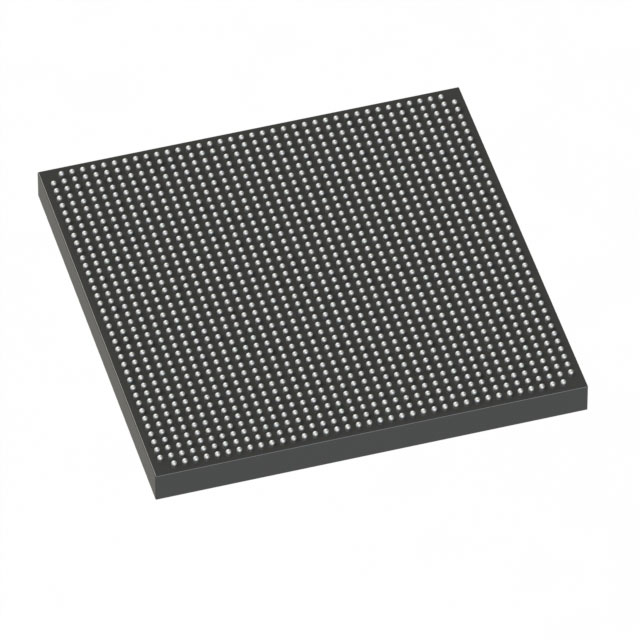
EP3SL340F1517I3G
| Part Description |
Field Programmable Gate Array (FPGA) IC |
|---|---|
| Quantity | 1,271 Available (as of October 7, 2026) |
| Product Category | Field Programmable Gate Array (FPGA) |
|---|---|
| Manufacturer | Intel |
| Manufacturing Status | Active |
| Manufacturer Standard Lead Time | 26 Weeks |
| Datasheet |
Specifications & Environmental
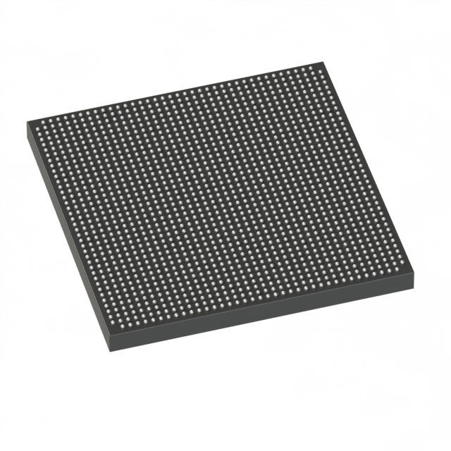
| Device Package | 1517-FBGA (40x40) | Grade | Industrial | Operating Temperature | -40°C – 100°C | ||
|---|---|---|---|---|---|---|---|
| Package / Case | 1517-BBGA, FCBGA | Number of I/O | 976 | Voltage | 860 mV - 1.15 V | ||
| Mounting Method | Surface Mount | RoHS Compliance | RoHS Compliant | REACH Compliance | REACH Unaffected | ||
| Moisture Sensitivity Level | 3 (168 Hours) | Number of LABs/CLBs | 13500 | Number of Logic Elements/Cells | 337500 | ||
| Number of Gates | N/A | ECCN | N/A | HTS Code | N/A | ||
| Qualification | N/A | Total RAM Bits | 18822144 |
Overview of EP3SL340F1517I3G – Field Programmable Gate Array (FPGA) IC
The EP3SL340F1517I3G is an Intel Stratix III family FPGA provided in a 1517‑FBGA surface‑mount package and specified for industrial grade use. It delivers a high logical capacity and significant embedded memory for demanding digital signal processing, high‑performance logic and embedded system integration.
Built on a 65‑nm, 1.1‑V SRAM process and incorporating family‑level features such as programmable power management, on‑chip security and robust high‑speed I/O support, this device targets applications that require large FPGA fabric, advanced DSP capability and reliable operation across –40 °C to 100 °C.
Key Features
- Logic Capacity Approximately 337,500 logic elements for complex custom logic, control and datapath implementations.
- Embedded Memory Approximately 18.8 Mbits of on‑chip RAM (18,822,144 total bits) to support large FIFOs, frame buffers and scratch memory.
- I/O and Packaging 976 user I/O in a 1517‑FBGA (40×40) package; surface‑mount package suitable for dense board layouts.
- Power and Core Voltage Core supply range 0.860 V to 1.15 V, enabling selectable operating points for performance versus power tradeoffs.
- Temperature and Grade Industrial grade device rated for operation from –40 °C to 100 °C.
- High‑Speed DSP Blocks Family‑level DSP architecture supports dedicated multipliers (9×9, 12×12, 18×18, 36×36) with performance up to 550 MHz for FIR, MAC and signal processing functions.
- Clocking and PLLs Family features include up to 16 global clocks, extensive regional/peripheral clocking and up to 12 PLLs for flexible clock synthesis and distribution.
- Security and Reliability Family‑level support for 256‑bit AES volatile/non‑volatile encryption of configuration bitstreams, CRC and ECC options for configuration and memory error detection/correction.
- Standards and Memory Interfaces Family supports high‑speed external memory interfaces (DDR/DDR2/DDR3, RLDRAM II, QDR II/II+) and modular I/O banks with dedicated DQS logic for memory timing.
- RoHS Compliant Environmentally compliant manufacturing and materials.
Typical Applications
- High‑Performance DSP Systems Use the large logic fabric and dedicated multipliers for real‑time signal processing, FIR filtering and algorithm acceleration.
- Network and Communications Leverage high‑speed SERDES, modular I/O banks and robust clocking to implement protocol processing, packet engines and interface bridging.
- Memory Interface Controllers Implement complex DDR/DDR2/DDR3 or QDR memory controllers using the device’s DQS logic and abundant on‑chip memory for buffering.
- Embedded Computing and Custom Logic Deploy extensive logic elements and embedded RAM for custom processors, accelerator engines and system glue logic in industrial systems.
Unique Advantages
- Massive Logic and Memory in One Device: Combine ~337,500 logic elements with ~18.8 Mbits of embedded RAM to consolidate complex systems and reduce external components.
- Flexible Performance vs. Power: Core supply range (0.860–1.15 V) and programmable power technology (family feature) allow designers to tune for power efficiency or higher throughput.
- Advanced DSP Capability: Dedicated wide multipliers and high‑frequency DSP paths enable efficient implementation of demanding signal processing tasks.
- Robust I/O and Memory Support: Nearly 1,000 user I/O and modular I/O bank architecture support high‑speed external memory and diverse interface standards.
- Security and Reliability Options: Family‑level AES encryption, CRC and ECC features help protect configuration integrity and maintain system availability.
Why Choose EP3SL340F1517I3G?
EP3SL340F1517I3G positions itself for systems requiring substantial on‑chip logic and memory resources, combined with advanced DSP and flexible I/O. Its industrial temperature rating and surface‑mount 1517‑FBGA package make it suitable for robust embedded and communications hardware where board density and thermal range matter.
Designers benefit from a well‑specified device platform that ties high logical capacity and embedded memory to family‑level reliability and security features, providing a scalable foundation for high‑performance, long‑lifecycle designs supported by Intel’s Stratix III architecture.
Request a quote or submit an inquiry for EP3SL340F1517I3G to receive pricing and availability information tailored to your project needs.





















Date Founded: 1968
Headquarters: Santa Clara, California, USA
Employees: 130,000+
Revenue: $54.23 Billion
Certifications and Memberships: ISO9001:2015, ISO14001:2015, ISO17025:2017, ISO27001:2022, ISO45001:2018, ISO50001:2018


