
EP3SL50F484C3N
| Part Description |
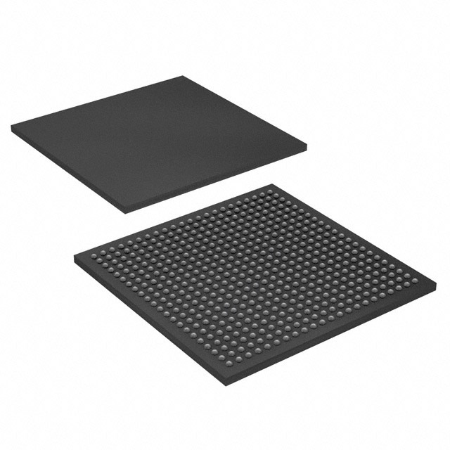
Stratix® III L Field Programmable Gate Array (FPGA) IC 296 2184192 47500 484-BBGA, FCBGA |
|---|---|
| Quantity | 1,421 Available (as of June 14, 2026) |

| Product Category | Field Programmable Gate Array (FPGA) |
|---|---|
| Manufacturer | Intel |
| Manufacturing Status | Obsolete |
| Manufacturer Standard Lead Time | Contact Us |
| Datasheet |
Specifications & Environmental
| Device Package | 484-FBGA (23x23) | Grade | Commercial | Operating Temperature | 0°C – 85°C | ||
|---|---|---|---|---|---|---|---|
| Package / Case | 484-BBGA, FCBGA | Number of I/O | 296 | Voltage | 860 mV - 1.15 V | ||
| Mounting Method | Surface Mount | RoHS Compliance | RoHS Compliant | REACH Compliance | REACH Unknown | ||
| Moisture Sensitivity Level | 3 (168 Hours) | Number of LABs/CLBs | 1900 | Number of Logic Elements/Cells | 47500 | ||
| Number of Gates | N/A | ECCN | 3A991D | HTS Code | 8542.39.0001 | ||
| Qualification | N/A | Total RAM Bits | 2184192 |
Overview of EP3SL50F484C3N – Stratix® III L FPGA, 484‑BBGA
The EP3SL50F484C3N is a Stratix III L field programmable gate array (FPGA) in a 484‑ball FCBGA (484‑BBGA) package. It implements the Stratix III device family architecture and provides a high‑density array of programmable logic, embedded memory, DSP resources and flexible I/O for complex digital designs.
Designed for commercial temperature operation, this device targets applications that require substantial logic capacity and on‑chip memory with a broad set of system features derived from the Stratix III family, including embedded memory blocks, DSP blocks, clock networks and high‑speed I/O structures.
Key Features
- Core Logic Approximately 47,500 logic elements (cells) delivering substantial programmable logic capacity for complex designs.
- Embedded Memory Approximately 2.18 Mbits of on‑chip RAM (2,184,192 total RAM bits) for data buffering, state storage and in‑FPGA memory structures.
- DSP and Processing Blocks Stratix III family DSP block architecture (as described in the device handbook) enables on‑chip arithmetic and signal processing acceleration.
- I/O Resources 296 user I/O pins suitable for a wide range of peripheral interfaces and external device connections; architecture supports high‑speed differential I/O structures per device documentation.
- Clocking and Timing Stratix III device family clock networks and PLL infrastructure provide flexible clock management and low‑jitter distribution (as documented in the device handbook).
- Package & Mounting 484‑BBGA FCBGA package (supplier package 484‑FBGA, 23×23) in a surface‑mount form factor for board‑level integration.
- Power Supply Range Core supply between 860 mV and 1.15 V to match system power architectures.
- Commercial Temperature Grade Rated for 0 °C to 85 °C operation and RoHS compliant.
- System Features (Series‑level) Device handbook highlights architecture elements such as TriMatrix embedded memory blocks, multiTrack interconnect, hot socketing and power‑on reset, configuration options, remote system upgrades and JTAG boundary‑scan support.
Typical Applications
- High‑performance data processing On‑chip DSP blocks and substantial logic density make this FPGA suitable for algorithm acceleration and real‑time signal processing tasks.
- High‑speed communications and protocol engines Support for high‑speed differential I/O and flexible clocking is suited to implementing protocol stacks, links and interface controllers.
- Memory interface controllers Extensive I/O and the Stratix III architecture support designs that interface with external memory and manage complex data paths.
- Custom embedded platforms Large logic capacity and embedded RAM allow integration of control, buffering and custom logic functions on a single FPGA device.
Unique Advantages
- High logic capacity: About 47,500 logic elements provide the headroom for complex, multi‑function designs without immediate need for multiple devices.
- Significant on‑chip memory: Approximately 2.18 Mbits of embedded RAM supports data buffering and stateful logic within the FPGA fabric.
- Comprehensive system features: Stratix III family architecture includes DSP blocks, TriMatrix memory, clock networks and configuration options documented in the device handbook, enabling integrated system designs.
- Flexible I/O count: 296 I/O pins allow connectivity to a wide range of peripherals and external components for diverse system topologies.
- Compact surface‑mount package: 484‑BBGA (23×23) FCBGA offers a compact footprint for high‑density PCBs and surface‑mount assembly.
- Commercial‑grade operation: Specified for 0 °C to 85 °C operation with RoHS compliance for standard commercial deployments.
Why Choose EP3SL50F484C3N?
The EP3SL50F484C3N places a large Stratix III L FPGA fabric, meaningful embedded memory and DSP capability into a compact 484‑BBGA surface‑mount package. It is positioned for designers who need substantial programmable logic and memory resources combined with flexible I/O and the architectural features documented for the Stratix III family.
This device suits projects that require integrated signal processing, complex protocol handling, or substantial on‑chip buffering while remaining within commercial temperature ranges. Designers benefit from the Stratix III family documentation and device‑level features to build scalable, well‑documented FPGA solutions.
Request a quote or submit an inquiry to obtain pricing, lead times and additional technical details for EP3SL50F484C3N.


Date Founded: 1968
Headquarters: Santa Clara, California, USA
Employees: 130,000+
Revenue: $54.23 Billion
Certifications and Memberships: ISO9001:2015, ISO14001:2015, ISO17025:2017, ISO27001:2022, ISO45001:2018, ISO50001:2018


