
EP3SL50F484C4LN
| Part Description |
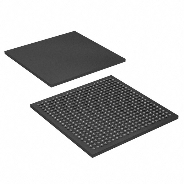
Stratix® III L Field Programmable Gate Array (FPGA) IC 296 2184192 47500 484-BBGA, FCBGA |
|---|---|
| Quantity | 1,254 Available (as of October 8, 2026) |
| Product Category | Field Programmable Gate Array (FPGA) |
|---|---|
| Manufacturer | Intel |
| Manufacturing Status | Obsolete |
| Manufacturer Standard Lead Time | Contact Us |
| Datasheet |
Specifications & Environmental
| Device Package | 484-FBGA (23x23) | Grade | Commercial | Operating Temperature | 0°C – 85°C | ||
|---|---|---|---|---|---|---|---|
| Package / Case | 484-BBGA, FCBGA | Number of I/O | 296 | Voltage | 860 mV - 1.15 V | ||
| Mounting Method | Surface Mount | RoHS Compliance | RoHS Compliant | REACH Compliance | REACH Unknown | ||
| Moisture Sensitivity Level | 3 (168 Hours) | Number of LABs/CLBs | 1900 | Number of Logic Elements/Cells | 47500 | ||
| Number of Gates | N/A | ECCN | 3A001A2C | HTS Code | 8542.39.0001 | ||
| Qualification | N/A | Total RAM Bits | 2184192 |
Overview of EP3SL50F484C4LN – Stratix® III L Field Programmable Gate Array (FPGA)
The EP3SL50F484C4LN is a Stratix® III L family FPGA in a 484‑ball BGA package optimized for commercial‑grade designs. It provides a high logic capacity FPGA fabric with embedded memory and a large I/O count for complex digital implementations.
With 47,500 logic elements, approximately 2.18 Mbits of on‑chip RAM, and 296 I/O pins, this device targets commercial systems that require substantial programmable logic, embedded memory, and flexible interfacing while operating within standard commercial temperature and voltage ranges.
Key Features
- Core Logic 47,500 logic elements for implementing complex digital logic and custom processing functions.
- Embedded Memory Approximately 2.18 Mbits of on‑chip RAM to support buffering, look‑up tables, and local data storage without external memory.
- I/O Capacity 296 general‑purpose I/O pins to interface with multiple peripherals, sensors, and external devices.
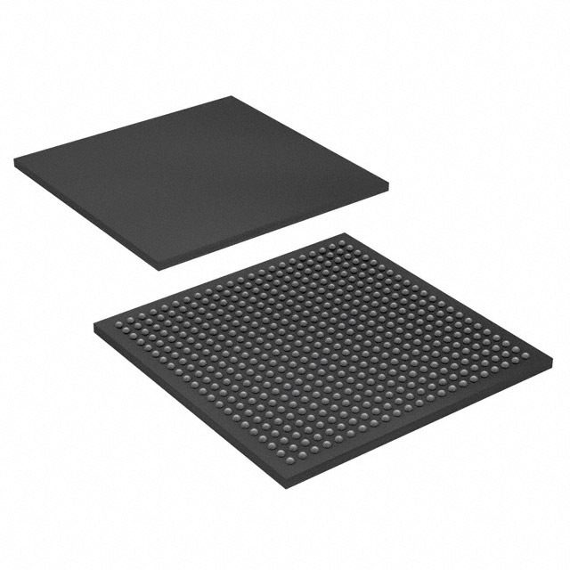
- Package 484‑BBGA (484‑FBGA, 23×23) FCBGA package providing a compact, high‑pin‑count footprint for space‑efficient board designs.
- Power Core supply voltage range from 0.860 V to 1.15 V for the FPGA core domain.
- Mounting and Compliance Surface‑mount device, RoHS compliant for regulatory and manufacturing compatibility.
- Commercial Temperature Range Rated for 0 °C to 85 °C operation suitable for commercial applications.
Typical Applications
- Commercial digital systems Use the device's 47,500 logic elements and 296 I/O to implement complex control, protocol handling, and custom logic in commercial equipment.
- Embedded memory‑intensive designs Leverage approximately 2.18 Mbits of on‑chip RAM for buffering, data tables, and real‑time processing without relying solely on external memory.
- High‑pin‑count board designs The 484‑ball FBGA package supports dense connectivity and compact board layouts where many signals need to be routed.
Unique Advantages
- High logic capacity: 47,500 logic elements enable substantial functional integration, reducing the need for multiple discrete components.
- Significant embedded memory: Approximately 2.18 Mbits of on‑chip RAM supports local data storage and accelerates data‑path operations.
- Extensive I/O: 296 I/O pins provide flexible interfacing for multi‑channel systems and complex peripheral integration.
- Compact, high‑density package: 484‑FBGA (23×23) simplifies layout for space‑constrained commercial designs while preserving connectivity.
- Commercial qualification: Rated for 0 °C to 85 °C, aligning with typical commercial environment requirements.
- Manufacturing compatibility: Surface‑mount BGA package and RoHS compliance support modern assembly and regulatory needs.
Why Choose EP3SL50F484C4LN?
The EP3SL50F484C4LN offers a balanced combination of high logic density, substantial embedded memory, and broad I/O capability in a compact 484‑ball FBGA package tailored for commercial applications. Its core voltage range and commercial temperature rating make it a practical choice for designs that require reliable programmable logic and on‑chip resources without extended environmental grading.
This device is well suited for developers and OEMs building commercial systems that demand integrated logic, local memory, and flexible interfacing while maintaining a compact board footprint and RoHS compliance. The on‑chip resources support scalable designs and help reduce board‑level complexity.
Request a quote or submit an inquiry to receive pricing and availability information for the EP3SL50F484C4LN. Include your required quantities and delivery timeframe to expedite a response.





















Date Founded: 1968
Headquarters: Santa Clara, California, USA
Employees: 130,000+
Revenue: $54.23 Billion
Certifications and Memberships: ISO9001:2015, ISO14001:2015, ISO17025:2017, ISO27001:2022, ISO45001:2018, ISO50001:2018


