
EP3SL50F780C4LG
| Part Description |
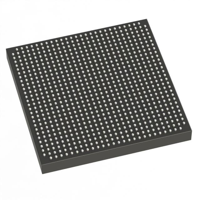
Stratix® III L Field Programmable Gate Array (FPGA) IC 488 2184192 47500 780-BBGA, FCBGA |
|---|---|
| Quantity | 1,060 Available (as of June 15, 2026) |

| Product Category | Field Programmable Gate Array (FPGA) |
|---|---|
| Manufacturer | Intel |
| Manufacturing Status | Active |
| Manufacturer Standard Lead Time | 26 Weeks |
| Datasheet |
Specifications & Environmental
| Device Package | 780-FBGA (29x29) | Grade | Commercial | Operating Temperature | 0°C – 85°C | ||
|---|---|---|---|---|---|---|---|
| Package / Case | 780-BBGA, FCBGA | Number of I/O | 488 | Voltage | 860 mV - 1.15 V | ||
| Mounting Method | Surface Mount | RoHS Compliance | RoHS Compliant | REACH Compliance | REACH Unaffected | ||
| Moisture Sensitivity Level | 3 (168 Hours) | Number of LABs/CLBs | 1900 | Number of Logic Elements/Cells | 47500 | ||
| Number of Gates | N/A | ECCN | PENDING ECCN | HTS Code | 0000.00.0000 | ||
| Qualification | N/A | Total RAM Bits | 2184192 |
Overview of EP3SL50F780C4LG – Stratix® III L Field Programmable Gate Array (FPGA) IC, 47,500 logic elements, 780-FBGA
The EP3SL50F780C4LG is a Stratix® III L family FPGA offering a balance of logic, embedded memory, and high‑speed I/O for high-performance digital designs. Built on the Stratix III architecture, it targets applications that require substantial programmable logic, on‑chip RAM, and flexible I/O in a 780‑ball FCBGA package.
This commercial‑grade, RoHS‑compliant device provides 47,500 logic elements, approximately 2.18 Mbits of embedded memory, and 488 user I/Os, with selectable core voltage and Programmable Power Technology for power/performance tradeoffs.
Key Features
- Programmable Logic — 47,500 logic elements (LEs) for implementing complex digital logic and control functions.
- On‑chip Memory — Approximately 2.18 Mbits of embedded RAM to support FIFOs, buffers, and memory‑centric functions.
- High‑Density I/O — 488 user I/Os arranged for modular banking and flexible interface support.
- Package & Mounting — 780‑FBGA (29×29) FCBGA package, surface‑mount for high‑density board designs.
- Core Voltage Range — Selectable core voltage operation from 0.86 V to 1.15 V to tune power and performance.
- Operating Range — Commercial operating temperature from 0 °C to 85 °C.
- Power Management — Programmable Power Technology (family feature) enables dynamic power/performance optimization by powering blocks only when needed.
- Clocking & Timing — Family support for multiple clock resources including up to 16 global clocks and up to 12 PLLs for clock synthesis and phase control.
- High‑Speed I/O Capabilities — Family‑level support for SERDES and dynamic phase alignment circuitry for high‑speed serial interfaces.
- Security & Reliability — Family options include AES configuration bitstream security and on‑chip error detection/correction features for enhanced reliability.
- Regulatory — RoHS compliant.
Typical Applications
- High‑Performance Logic & Control — Implement complex control engines, state machines, and custom logic for communications or industrial equipment using abundant logic elements.
- Digital Signal Processing — Deploy DSP functions and data‑path processing with integrated on‑chip RAM and dense logic resources.
- Memory Interface & Buffering — Use embedded RAM and modular I/O banks for memory controllers, buffering, and interface bridging.
- Networking & Communications — Implement packet processing, protocol logic, and serial interfaces leveraging high‑speed I/O and clocking resources.
Unique Advantages
- High Logic Capacity: 47,500 logic elements permit implementation of substantial custom logic without external ASICs.
- Significant Embedded Memory: Approximately 2.18 Mbits of on‑chip RAM reduces external memory reliance for many buffering and storage tasks.
- Flexible Power/Performance: Selectable core voltage and Programmable Power Technology allow designers to tune the device for power or performance as required.
- Dense I/O in a Compact Package: 488 user I/Os in a 780‑FBGA (29×29) package help minimize PCB area while supporting a variety of interfaces.
- Commercial‑Grade Reliability: Designed for 0 °C to 85 °C operation and RoHS compliance for mainstream electronics applications.
- Ecosystem & Integration: Family support includes embedded processor and megafunction options to accelerate system integration and IP reuse.
Why Choose EP3SL50F780C4LG?
The EP3SL50F780C4LG positions itself as a balanced, high‑capacity FPGA for designers who need substantial logic, embedded memory, and flexible I/O in a commercial‑grade device. Its selectable core voltage and family Programmable Power Technology enable tradeoffs between power consumption and performance to match target system requirements.
This Stratix III L device is suited to teams developing high‑performance digital, DSP, and communications designs that benefit from on‑chip RAM, extensive I/O, and advanced clocking and SERDES capabilities, with the option to leverage family‑level security and reliability features.
Request a quote or submit an inquiry to get pricing and availability for EP3SL50F780C4LG and to discuss how this Stratix® III L FPGA can fit your next design.


Date Founded: 1968
Headquarters: Santa Clara, California, USA
Employees: 130,000+
Revenue: $54.23 Billion
Certifications and Memberships: ISO9001:2015, ISO14001:2015, ISO17025:2017, ISO27001:2022, ISO45001:2018, ISO50001:2018


