
EP3SL70F484C2G
| Part Description |
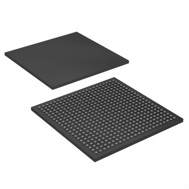
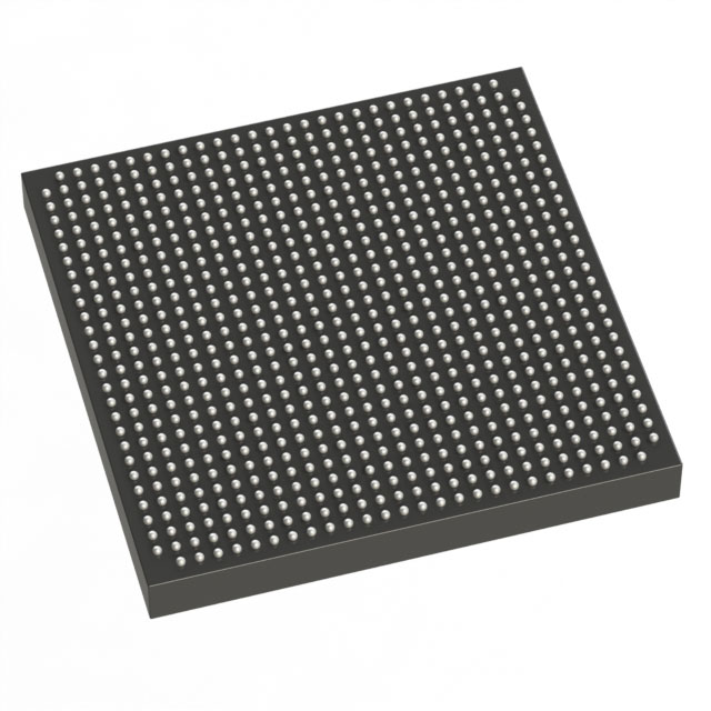
Stratix® III L Field Programmable Gate Array (FPGA) IC 296 2699264 67500 484-BBGA, FCBGA |
|---|---|
| Quantity | 27 Available (as of June 14, 2026) |

| Product Category | Field Programmable Gate Array (FPGA) |
|---|---|
| Manufacturer | Intel |
| Manufacturing Status | Active |
| Manufacturer Standard Lead Time | 26 Weeks |
| Datasheet |
Specifications & Environmental
| Device Package | 484-FBGA (23x23) | Grade | Commercial | Operating Temperature | 0°C – 85°C | ||
|---|---|---|---|---|---|---|---|
| Package / Case | 484-BBGA, FCBGA | Number of I/O | 296 | Voltage | 860 mV - 1.15 V | ||
| Mounting Method | Surface Mount | RoHS Compliance | RoHS Compliant | REACH Compliance | REACH Unaffected | ||
| Moisture Sensitivity Level | 3 (168 Hours) | Number of LABs/CLBs | 2700 | Number of Logic Elements/Cells | 67500 | ||
| Number of Gates | N/A | ECCN | PENDING ECCN | HTS Code | 0000.00.0000 | ||
| Qualification | N/A | Total RAM Bits | 2699264 |
Overview of EP3SL70F484C2G – Stratix® III L FPGA, 484-FBGA
The EP3SL70F484C2G is a Stratix III L field-programmable gate array (FPGA) offered in a 484-FBGA (23×23) surface-mount package. The device provides a balanced mix of logic, embedded memory and DSP capability targeted at high-performance logic, digital signal processing and embedded system integration.
With 67,500 logic elements, approximately 2.7 Mbits of embedded RAM and 296 user I/O pins, this commercial-grade FPGA is suited for applications that require significant on-chip resources, flexible high-speed I/O and selectable core-voltage power scaling for performance versus efficiency trade-offs.
Key Features
- Logic Capacity — 67,500 logic elements for implementing complex combinational and sequential logic functions.
- Embedded Memory — Approximately 2.7 Mbits of on-chip RAM for frame buffers, FIFOs and other memory-intensive functions.
- High-speed DSP Support — Family-level DSP resources support dedicated multipliers (including 9×9, 12×12, 18×18 and 36×36 configurations) for multiply-accumulate and FIR filtering workloads at high clock rates.
- I/O and SERDES — 296 user I/O pins with modular I/O bank architecture, dynamic on-chip termination and high-speed differential I/O with SERDES/DPA circuitry supporting up to 1.6 Gbps signaling.
- Clocking and PLLs — Rich clocking resources with up to 16 global clocks, 88 regional clocks, 116 peripheral clocks and up to 12 phase-locked loops (PLLs) for flexible clock synthesis and distribution.
- Security and Reliability — Device-family support for 256-bit AES volatile and non-volatile configuration key options, CRC for configuration memory error detection and ECC protection for embedded memory blocks.
- Power and Voltage — Programmable Power Technology and selectable core voltage operation with a supply range of 860 mV to 1.15 V to balance performance and power consumption.
- Package and Grade — Surface-mount 484-BBGA (FCBGA) package (484-FBGA, 23×23); commercial temperature grade with an operating range of 0 °C to 85 °C. RoHS compliant.
Typical Applications
- High-performance signal processing — Implement FIR filters, FFTs and other DSP-heavy functions using the device’s dedicated multiplier blocks and abundant logic resources.
- Networking and communications — Use the high-speed differential I/O, SERDES and modular I/O banks for protocol implementation and packet processing at multi-gigabit interfaces.
- Memory interface controllers — Support for external memory interfaces (DDR/DDR2/DDR3 and other high-speed memories at the family level) combined with large on-chip RAM for buffering and timing-critical designs.
- Embedded systems and custom logic — Leverage the large logic element count and clocking resources to implement custom processors, accelerators and control logic within a single device footprint.
Unique Advantages
- Balanced resource mix: 67,500 logic elements and approximately 2.7 Mbits of embedded RAM deliver a mid-to-high density FPGA architecture suitable for combined logic and memory workloads.
- Flexible high-speed I/O: 296 user I/O and SERDES/DPA support enable diverse interface options and reliable signal integrity for high-bandwidth designs.
- Advanced clocking: Extensive global/regional/peripheral clocks and up to 12 PLLs simplify multi-clock-domain designs and clock synthesis requirements.
- Configurable power/performance: Selectable core voltage and programmable power features allow designers to tune the device for higher performance or lower power consumption.
- Security and data integrity: Support for 256-bit AES configuration keys, CRC for configuration memory and ECC for embedded RAM enhance design protection and runtime reliability.
- Commercial-grade package: Surface-mount 484-FBGA package provides a compact, manufacturable footprint for high-density system integration.
Why Choose EP3SL70F484C2G?
The EP3SL70F484C2G is positioned for designers who need a flexible, high-capacity FPGA with a balanced combination of logic, memory and DSP resources. Its extensive clocking and PLL options, robust I/O capabilities and configurable power modes make it well suited for demanding embedded, signal-processing and communications applications.
Choosing this Stratix III L device delivers a scalable platform with on-chip security and error-detection features that support long-term design robustness and system-level reliability, while the commercial-grade package and RoHS compliance simplify integration into mainstream product lines.
Request a quote or submit an inquiry to receive pricing, availability and technical assistance for EP3SL70F484C2G.


Date Founded: 1968
Headquarters: Santa Clara, California, USA
Employees: 130,000+
Revenue: $54.23 Billion
Certifications and Memberships: ISO9001:2015, ISO14001:2015, ISO17025:2017, ISO27001:2022, ISO45001:2018, ISO50001:2018


