
EP3SL70F484C3N
| Part Description |
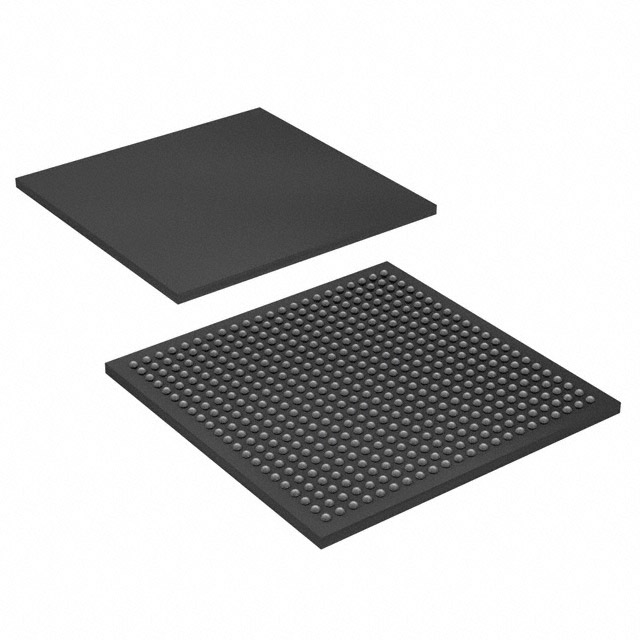
Stratix® III L Field Programmable Gate Array (FPGA) IC 296 2699264 67500 484-BBGA, FCBGA |
|---|---|
| Quantity | 1,486 Available (as of June 14, 2026) |

| Product Category | Field Programmable Gate Array (FPGA) |
|---|---|
| Manufacturer | Intel |
| Manufacturing Status | Obsolete |
| Manufacturer Standard Lead Time | Contact Us |
| Datasheet |
Specifications & Environmental
| Device Package | 484-FBGA (23x23) | Grade | Commercial | Operating Temperature | 0°C – 85°C | ||
|---|---|---|---|---|---|---|---|
| Package / Case | 484-BBGA, FCBGA | Number of I/O | 296 | Voltage | 860 mV - 1.15 V | ||
| Mounting Method | Surface Mount | RoHS Compliance | RoHS Compliant | REACH Compliance | REACH Unknown | ||
| Moisture Sensitivity Level | 3 (168 Hours) | Number of LABs/CLBs | 2700 | Number of Logic Elements/Cells | 67500 | ||
| Number of Gates | N/A | ECCN | 3A991D | HTS Code | 8542.39.0001 | ||
| Qualification | N/A | Total RAM Bits | 2699264 |
Overview of EP3SL70F484C3N – Stratix® III L Field Programmable Gate Array (FPGA) IC
The EP3SL70F484C3N is a Stratix® III L FPGA supplied in a 484-BBGA (FCBGA) surface-mount package. The device integrates 67,500 logic elements and approximately 2.7 Mbits of embedded memory, making it suitable for complex digital designs that require large logic capacity and on-chip RAM.
Designed for commercial-grade systems, the device provides 296 user I/O pins, programmable power options and support for high-speed I/O and DSP-oriented functions as detailed in the Stratix III device documentation. Typical system use cases include communications, high-performance signal processing, and embedded interface/control implementations.
Key Features
- Core Logic 67,500 logic elements (cells) for implementing large, high-density digital designs.
- Embedded Memory Approximately 2.7 Mbits of on-chip RAM organized in TriMatrix embedded memory blocks for buffering, FIFOs and packet or data storage.
- I/O and Interfaces 296 device I/O pins and architecture-level support for high-speed differential I/O interfaces and external memory interfaces as described in the Stratix III family documentation.
- DSP and Timing Device family features include DSP blocks and comprehensive clock networks with PLLs for synchronous, high-throughput signal processing (see device handbook).
- Configuration and Test Supports standard configuration schemes and IEEE 1149.1 (JTAG) boundary-scan testing for board-level validation and in-system programming.
- Power Specified core voltage supply range of 0.86 V to 1.15 V and programmable power options referenced in the device handbook.
- Package and Mounting 484-BBGA FCBGA package (supplier device package: 484-FBGA, 23×23); surface-mount for compact board integration.
- Operating Range and Grade Commercial grade operation with an operating temperature range of 0 °C to 85 °C; RoHS compliant.
Typical Applications
- Communications Infrastructure Implements protocol processing, packet handling and interface bridging using the device’s high I/O count and on-chip memory.
- High-Performance Signal Processing Leverages DSP blocks, clock networks and abundant logic elements for filtering, FFTs and real-time compute tasks.
- Embedded Systems and Prototyping Supports complex control logic, custom peripherals and system integration in compact FCBGA form factors.
- Memory Interface Controllers Enables external memory interface designs and buffering logic using embedded memory and dedicated I/O resources.
Unique Advantages
- High Logic Density: 67,500 logic elements provide capacity for complex state machines, datapaths and custom accelerators without external glue logic.
- Substantial On-Chip Memory: Approximately 2.7 Mbits of embedded RAM reduce dependency on external memory for buffering and temporary storage.
- Extensive I/O: 296 I/O pins support wide parallel interfaces and multiple high-speed serial/differential channels when used with the device family I/O features.
- Package Efficiency: 484-BBGA (FCBGA) surface-mount package enables compact board layouts and high pin density in a 23×23 supplier package footprint.
- Documented Platform: Part of the Stratix III family with comprehensive device handbook content covering architecture, DSP blocks, clocking, configuration and I/O capabilities.
- Commercial Readiness: Commercial-grade temperature rating (0 °C to 85 °C) and RoHS compliance support mainstream production and deployment.
Why Choose EP3SL70F484C3N?
The EP3SL70F484C3N positions itself as a high-capacity Stratix III L FPGA option for designers who need a balance of large programmable logic, substantial on-chip RAM and a high I/O count in a compact FCBGA package. Its documented family features—DSP blocks, advanced clock networks, and configurable I/O—help designers implement demanding digital and signal-processing applications.
This device is suited for teams building communications equipment, compute-accelerated embedded systems or memory-interface controllers who require a commercially rated, RoHS-compliant FPGA backed by the Stratix III device handbook and family documentation for design guidance and system integration.
Request a quote or submit an inquiry to learn about availability, pricing and lead times for the EP3SL70F484C3N.


Date Founded: 1968
Headquarters: Santa Clara, California, USA
Employees: 130,000+
Revenue: $54.23 Billion
Certifications and Memberships: ISO9001:2015, ISO14001:2015, ISO17025:2017, ISO27001:2022, ISO45001:2018, ISO50001:2018


