
EP4SE230F29C3G
| Part Description |
Field Programmable Gate Array (FPGA) IC |
|---|---|
| Quantity | 457 Available (as of June 15, 2026) |

| Product Category | Field Programmable Gate Array (FPGA) |
|---|---|
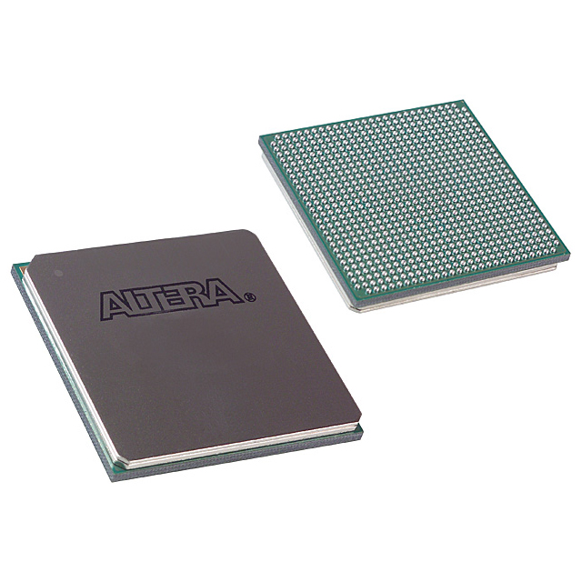
| Manufacturer | Intel |
| Manufacturing Status | Active |
| Manufacturer Standard Lead Time | 26 Weeks |
| Datasheet |
Specifications & Environmental
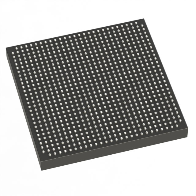
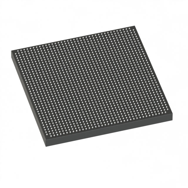
| Device Package | 780-FBGA (29x29) | Grade | Commercial | Operating Temperature | 0°C – 85°C | ||
|---|---|---|---|---|---|---|---|
| Package / Case | 780-BGA | Number of I/O | 488 | Voltage | 870 mV - 930 mV | ||
| Mounting Method | Surface Mount | RoHS Compliance | RoHS Compliant | REACH Compliance | REACH Unaffected | ||
| Moisture Sensitivity Level | 3 (168 Hours) | Number of LABs/CLBs | 9120 | Number of Logic Elements/Cells | 228000 | ||
| Number of Gates | N/A | ECCN | N/A | HTS Code | N/A | ||
| Qualification | N/A | Total RAM Bits | 17544192 |
Overview of EP4SE230F29C3G – Field Programmable Gate Array (FPGA) IC
The EP4SE230F29C3G is an Intel Stratix IV family Field Programmable Gate Array (FPGA) IC optimized for high-capacity logic and system integration. It combines a large logic fabric with substantial on-chip memory and a broad set of I/O to support data‑intensive, protocol‑aware, and DSP‑oriented designs.
Designed for commercial‑grade applications, this device targets customers building high‑throughput data paths, external memory interfaces, and complex system logic requiring flexible, reconfigurable silicon with documented Stratix IV architecture features.
Key Features
- Core Logic: 228,000 logic elements (cells) provide significant programmable logic capacity for complex mapping and parallel processing.
- Embedded Memory: Approximately 17.5 Mbits of on‑chip RAM to support buffering, FIFOs, and DSP data storage within the device fabric.
- I/O Resources: 488 I/O pins enable dense connectivity to peripherals, external memory, and high‑speed interfaces.
- Stratix IV Architecture Highlights: Device documentation references integrated architecture features such as high‑speed transceivers, DSP blocks, PLLs and extensive clock networks for system timing and signal management.
- Power Supply Range: Operates from 870 mV to 930 mV supply rails, enabling defined power sequencing and system integration planning.
- Package & Mounting: 780‑FBGA package (29 × 29) in a 780‑BGA footprint, designed for surface‑mount assembly.
- Commercial Temperature Grade: Rated for operation from 0 °C to 85 °C and provided as RoHS compliant.
Typical Applications
- High‑Throughput Networking: Use for protocol handling and data routing where a large logic fabric and extensive I/O are required.
- Signal Processing and DSP: On‑chip RAM combined with documented DSP block capability supports streaming and real‑time signal processing tasks.
- External Memory Interfaces: Suitable for designs that bridge or control external memory subsystems, leveraging the device’s memory interface features.
- System Integration and Prototyping: Reconfigurable fabric and comprehensive clocking/PLL resources make the device a fit for system integration, prototyping, and complex control logic.
Unique Advantages
- High Logic Capacity: 228,000 logic elements enable implementation of large, parallelized designs without immediate up‑scope to multiple devices.
- Significant Embedded Memory: Approximately 17.5 Mbits of on‑chip RAM reduces external memory dependence for buffering and local data storage.
- Wide I/O Count: 488 I/O pins allow flexible interfacing to a variety of peripherals and external subsystems, simplifying board routing and integration.
- Documented Stratix IV Feature Set: Architecture documentation highlights high‑speed transceivers, PLLs, DSP blocks and clock network resources to support timing‑sensitive designs.
- Commercial‑Grade Specification: 0 °C to 85 °C operating range and RoHS compliance make it suitable for mainstream commercial products and assemblies.
- Standard Surface‑Mount Package: 780‑FBGA (29 × 29) package supports common PCB assembly processes for compact, high‑density layouts.
Why Choose EP4SE230F29C3G?
The EP4SE230F29C3G positions itself as a high‑capacity Stratix IV FPGA option for engineers needing large logic resources, substantial embedded memory, and extensive I/O in a commercial‑grade device. Its documented architecture features—such as transceivers, DSP resources, PLLs and clock networks—support designs that require precise timing and data throughput management.
This device is well suited to teams developing high‑bandwidth data paths, DSP‑heavy subsystems, and advanced system integration projects that benefit from a reprogrammable, vendor‑documented FPGA platform backed by Intel’s Stratix IV family documentation.
If you would like pricing, lead‑time information, or to request a formal quote for EP4SE230F29C3G, please submit a request or quote inquiry and our team will respond with details.


Date Founded: 1968
Headquarters: Santa Clara, California, USA
Employees: 130,000+
Revenue: $54.23 Billion
Certifications and Memberships: ISO9001:2015, ISO14001:2015, ISO17025:2017, ISO27001:2022, ISO45001:2018, ISO50001:2018


