
EP4SE530F43C3ES
| Part Description |
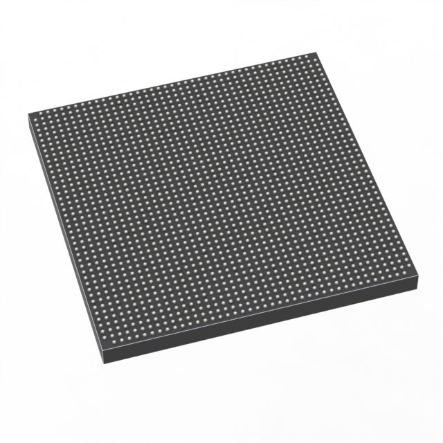
STRATIX® IV E Field Programmable Gate Array (FPGA) IC 1120 28033024 531200 1760-BBGA, FCBGA |
|---|---|
| Quantity | 285 Available (as of October 8, 2026) |

| Product Category | Field Programmable Gate Array (FPGA) |
|---|---|
| Manufacturer | Intel |
| Manufacturing Status | Obsolete |
| Manufacturer Standard Lead Time | Contact Us |
| Datasheet |
Specifications & Environmental
| Device Package | 1760-FCBGA (42.5x42.5) | Grade | Commercial | Operating Temperature | 0°C – 85°C | ||
|---|---|---|---|---|---|---|---|
| Package / Case | 1760-BBGA, FCBGA | Number of I/O | 1120 | Voltage | 870 mV - 930 mV | ||
| Mounting Method | Surface Mount | RoHS Compliance | RoHS non-compliant | REACH Compliance | REACH Unaffected | ||
| Moisture Sensitivity Level | 3 (168 Hours) | Number of LABs/CLBs | 21248 | Number of Logic Elements/Cells | 531200 | ||
| Number of Gates | N/A | ECCN | 3A001A7A | HTS Code | 8542.39.0001 | ||
| Qualification | N/A | Total RAM Bits | 28033024 |
Overview of EP4SE530F43C3ES – STRATIX® IV E Field Programmable Gate Array (FPGA) IC
The EP4SE530F43C3ES is a Stratix® IV E field programmable gate array offering a high-density programmable fabric and system integration features drawn from the Stratix IV device family. Its architecture provides a large number of logic elements, substantial on-chip memory, and extensive I/O to support complex digital designs.
Designed for commercial-grade applications, this device targets high-bandwidth data processing, signal processing and system integration use cases where high logic capacity, abundant embedded memory, and flexible I/O are required.
Key Features
- Core Logic — 531,200 logic elements provide substantial programmable capacity for complex designs and large-scale logic integration.
- Embedded Memory — Approximately 28 Mbits of on-chip RAM (28,033,024 total RAM bits) to support buffers, FIFOs and local storage without external memory.
- I/O Density — 1,120 I/O pins to interface with high-pin-count peripherals, parallel buses and multi-channel systems.
- Device Family Features — Stratix IV E family architecture features such as embedded DSP blocks, clock networks, PLLs, and support for high-speed I/O and external memory interfaces as described in the device handbook.
- Power — Core voltage supply range of 870 mV to 930 mV to match system power-rail design and power budgeting requirements.
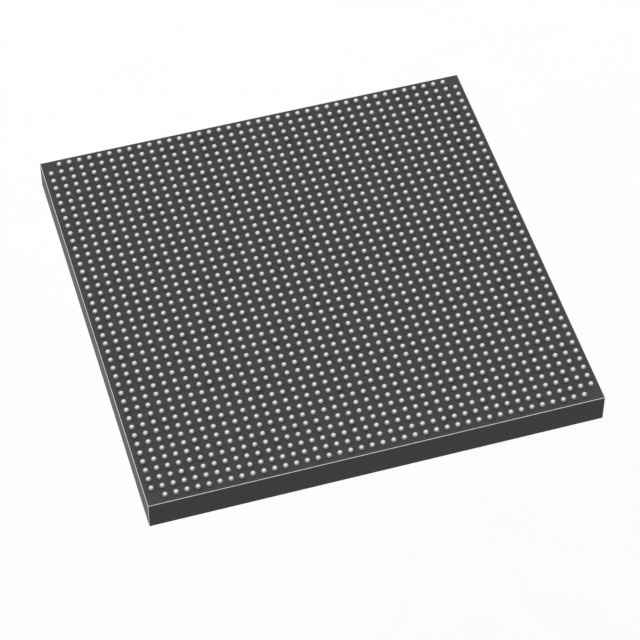
- Package & Mounting — 1760-FCBGA (1760-BBGA) surface-mount package with dimensions 42.5 × 42.5 mm for dense board-level integration.
- Operating Range — Commercial operating temperature range of 0 °C to 85 °C.
- Environmental Compliance — RoHS compliant.
Typical Applications
- High-bandwidth networking and telecom — Use the device’s architecture and high I/O count to implement packet processing, protocol bridging and interface aggregation where aggregate data bandwidth and I/O density are important.
- Digital signal processing and video — Leverage embedded DSP blocks and on-chip memory for real-time filtering, codec functions and multi-channel signal pipelines.
- Memory-interface systems — Implement external memory interfaces and buffering schemes using the device’s clocking resources, PLLs and embedded RAM.
- System integration and prototyping — Integrate multiple subsystems and custom logic into a single FPGA to reduce board-level component count and accelerate system-level validation.
Unique Advantages
- High programmable capacity: 531,200 logic elements enable integration of large, complex designs on a single device.
- Substantial on-chip memory: Approximately 28 Mbits of embedded RAM reduces dependence on external memory for many buffering and storage tasks.
- Extensive I/O connectivity: 1,120 I/O pins accommodate multiple high-pin-count interfaces and parallel data channels.
- Compact, high-density package: 1760-FCBGA (42.5 × 42.5 mm) offers a compact footprint for high-density system boards while supporting surface-mount assembly.
- Power-rail flexibility: Core voltage range of 870 mV–930 mV supports modern low-voltage power architectures.
- Commercial-grade readiness: Specified operating range of 0 °C–85 °C and RoHS compliance match common commercial deployment requirements.
Why Choose EP4SE530F43C3ES?
The EP4SE530F43C3ES combines a high logic-element count, large embedded memory capacity and a very high I/O count within the Stratix IV E device family architecture. That combination makes it well suited for designers who need to consolidate complex logic, DSP functions and multi-channel interfaces into a single FPGA package while maintaining commercial operating specifications.
For teams focused on scalable, board-level integration and rapid system prototyping, this device delivers the programmable resources and package density needed to shorten development cycles and simplify BOMs, backed by the Stratix IV family technical features documented in the device handbook.
Request a quote or submit an inquiry for pricing and availability to evaluate EP4SE530F43C3ES for your next design.
























Date Founded: 1968
Headquarters: Santa Clara, California, USA
Employees: 130,000+
Revenue: $54.23 Billion
Certifications and Memberships: ISO9001:2015, ISO14001:2015, ISO17025:2017, ISO27001:2022, ISO45001:2018, ISO50001:2018


