
EP4SE530F43C3G
| Part Description |
Field Programmable Gate Array (FPGA) IC |
|---|---|
| Quantity | 1,046 Available (as of June 15, 2026) |

| Product Category | Field Programmable Gate Array (FPGA) |
|---|---|
| Manufacturer | Intel |
| Manufacturing Status | Active |
| Manufacturer Standard Lead Time | 8 Weeks |
| Datasheet |
Specifications & Environmental
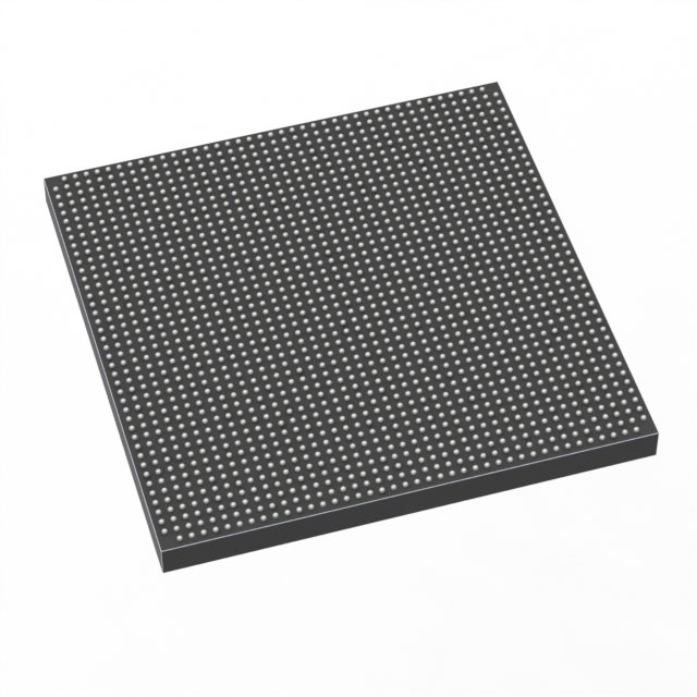
| Device Package | 1760-FCBGA (42.5x42.5) | Grade | Commercial | Operating Temperature | 0°C – 85°C | ||
|---|---|---|---|---|---|---|---|
| Package / Case | 1760-BBGA, FCBGA | Number of I/O | 1120 | Voltage | 870 mV - 930 mV | ||
| Mounting Method | Surface Mount | RoHS Compliance | RoHS Compliant | REACH Compliance | REACH Unaffected | ||
| Moisture Sensitivity Level | 3 (168 Hours) | Number of LABs/CLBs | 21248 | Number of Logic Elements/Cells | 531200 | ||
| Number of Gates | N/A | ECCN | N/A | HTS Code | N/A | ||
| Qualification | N/A | Total RAM Bits | 28033024 |
Overview of EP4SE530F43C3G – Field Programmable Gate Array (FPGA) IC
The EP4SE530F43C3G is a Stratix IV-family Field Programmable Gate Array (FPGA) IC from Intel. It delivers high logic density and on-chip memory paired with a large I/O count for designs that require complex custom logic, embedded memory, and extensive interfacing.
Built on the Stratix IV device architecture, the device targets applications that benefit from integrated DSP features, high-speed transceiver and external memory interface support as described in the device handbook. The part is offered in a high-pin-count FCBGA package for surface-mount system integration.
Key Features
- Core logic — 531,200 logic elements (cells) to implement large-scale programmable logic and custom processing pipelines.
- Embedded memory — Approximately 28 Mbits of on-chip RAM (28,033,024 bits) for buffering, frame storage, and data-path acceleration.
- I/O density — 1,120 I/O pins to support broad external interfacing and parallel connections.
- Stratix IV architecture — Device family features include DSP blocks, PLLs, clock networks, high-speed transceiver support, and external memory interface capabilities as documented in the Stratix IV device handbook.
- Package & mounting — 1760-FCBGA (1760-BBGA) surface-mount package, 42.5 × 42.5 mm footprint for board-level integration.
- Power — Core voltage supply range of 870 mV to 930 mV for the device core domain.
- Temperature & grade — Commercial grade operation with an operating temperature range of 0 °C to 85 °C.
- Compliance — RoHS compliant.
Typical Applications
- High-speed networking and communications — Leverages Stratix IV high-speed transceiver and bandwidth-focused architecture to support protocol and data-path implementations that require large aggregate throughput.
- Digital signal processing — Large logic element count and substantial embedded memory make the device suitable for DSP-intensive tasks such as filtering, encoding/decoding, and real-time data manipulation.
- Memory interface controllers — Designed to support external memory interfaces and on-chip RAM for controllers, buffering and complex memory arbitration logic.
- Custom hardware acceleration — High logic density and extensive I/O enable offloading compute-heavy kernels and creating dedicated acceleration blocks for system-level performance.
Unique Advantages
- High integration density: 531,200 logic elements and ~28 Mbits of embedded memory reduce the need for external logic and memory chips, simplifying board BOM and layout.
- Broad interfacing capability: 1,120 I/O pins and the FCBGA footprint provide flexibility for connecting high-pin-count peripherals and parallel interfaces.
- Stratix IV architecture benefits: Family-level features such as DSP blocks, PLLs, and high-speed transceiver support enable complex signal processing and timing architectures.
- Low-voltage core operation: Core supply range of 870–930 mV supports the device’s core power requirements and system power planning.
- RoHS compliant: Meets environmental compliance requirements for lead-free manufacturing processes.
Why Choose EP4SE530F43C3G?
The EP4SE530F43C3G positions itself as a high-density, feature-rich Stratix IV FPGA option for designs requiring substantial programmable logic, embedded memory, and I/O capacity. Its combination of logic elements, on-chip RAM and family-level architecture features supports applications spanning high-throughput communications, DSP acceleration, and complex memory interfacing.
Engineers and system designers benefit from the device handbook and Stratix IV family documentation when planning integration, timing and system-level architectures, providing a clear path for scalable implementations using this device.
Request a quote or submit an inquiry for pricing and availability of EP4SE530F43C3G to receive further technical and procurement information.


Date Founded: 1968
Headquarters: Santa Clara, California, USA
Employees: 130,000+
Revenue: $54.23 Billion
Certifications and Memberships: ISO9001:2015, ISO14001:2015, ISO17025:2017, ISO27001:2022, ISO45001:2018, ISO50001:2018


