
EP4SGX110DF29C2XN
| Part Description |
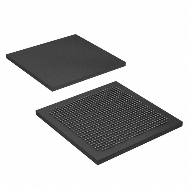
Stratix® IV GX Field Programmable Gate Array (FPGA) IC 372 9793536 105600 780-BBGA, FCBGA |
|---|---|
| Quantity | 1,829 Available (as of October 8, 2026) |

| Product Category | Field Programmable Gate Array (FPGA) |
|---|---|
| Manufacturer | Intel |
| Manufacturing Status | Obsolete |
| Manufacturer Standard Lead Time | Contact Us |
| Datasheet |
Specifications & Environmental
| Device Package | 780-FBGA (29x29) | Grade | Commercial | Operating Temperature | 0°C – 85°C | ||
|---|---|---|---|---|---|---|---|
| Package / Case | 780-BBGA, FCBGA | Number of I/O | 372 | Voltage | 870 mV - 930 mV | ||
| Mounting Method | Surface Mount | RoHS Compliance | RoHS Compliant | REACH Compliance | REACH Unknown | ||
| Moisture Sensitivity Level | 3 (168 Hours) | Number of LABs/CLBs | 4224 | Number of Logic Elements/Cells | 105600 | ||
| Number of Gates | N/A | ECCN | 3A991D | HTS Code | 8542.39.0001 | ||
| Qualification | N/A | Total RAM Bits | 9793536 |
Overview of EP4SGX110DF29C2XN – Stratix® IV GX FPGA, 105,600 logic elements
The EP4SGX110DF29C2XN is a Stratix® IV GX field programmable gate array (FPGA) IC from Intel, offering a high-density programmable fabric packaged in a 780‑FBGA (29×29) FCBGA. It delivers 105,600 logic elements, approximately 9.79 Mbits of embedded memory, and 372 general-purpose I/O pins for complex, memory- and I/O‑intensive FPGA designs.
Device-level documentation for the Stratix IV family includes detailed DC and switching characteristics, transceiver and PLL specifications, DSP block and TriMatrix memory block specifications, and configuration/JTAG information to support design and integration.
Key Features
- Core Logic Provides 105,600 logic elements suitable for large, high‑density programmable designs.
- Embedded Memory Approximately 9.79 Mbits of on‑chip RAM to support buffering, lookup tables, and embedded data storage.
- I/O and Interfaces 372 user I/O pins with documented I/O standard specifications and transceiver performance guidance in the device handbook.
- Programmable DSP Resources Device handbook includes DSP block specifications for signal processing and arithmetic acceleration.
- Clocking and Timing Comprehensive clock tree and PLL specifications are provided in the Stratix IV device documentation for clock management and low-latency datapaths.
- Configuration and Debug Configuration and JTAG specifications are provided to streamline programming, debugging, and manufacturing test.
- Package and Mounting 780‑BBGA / 780‑FBGA (29×29) FCBGA package in a surface‑mount form factor for compact board designs.
- Power Operates from a supply range of 870 mV to 930 mV; refer to the device handbook for detailed power consumption guidance and recommended operating conditions.
- Temperature & Grade Commercial grade device with an operating temperature range of 0 °C to 85 °C.
- Regulatory RoHS compliant.
Typical Applications
- High‑density digital processing Deploy the FPGA fabric and DSP block resources for complex custom logic, algorithm acceleration, and large-scale state machines.
- High‑speed serial and parallel interfaces Use the documented transceiver and I/O specifications to implement multi‑lane serial links and wide parallel interfaces.
- Memory‑intensive accelerators Embedded RAM capacity supports buffering, packet queuing, and local data storage for streaming and packet processing designs.
- Compact system integration The 780‑FBGA 29×29 surface‑mount package enables dense board layouts for space‑constrained FPGA-based modules and appliances.
Unique Advantages
- High logic density: 105,600 logic elements reduce the need for multi‑chip implementations in complex designs.
- Substantial on‑chip memory: Approximately 9.79 Mbits of embedded RAM supports large buffering and state storage without external memory in many applications.
- Extensive I/O capacity: 372 user I/O pins allow flexible interfacing to peripherals, sensors, and high‑speed links.
- Comprehensive device documentation: The Stratix IV device handbook provides DC/switching characteristics, PLL, transceiver, DSP, TriMatrix memory, and configuration/JTAG details to aid design and validation.
- Compact FCBGA package: 780‑FBGA (29×29) surface‑mount footprint supports higher board density and reliable solder attachment.
- Manufacturing compliance: RoHS compliance supports environmentally conscious production processes.
Why Choose EP4SGX110DF29C2XN?
The EP4SGX110DF29C2XN positions itself as a high‑density Stratix IV GX FPGA for designs that require substantial logic capacity, significant embedded memory, and large I/O counts in a compact FCBGA package. Detailed device documentation covering power, timing, transceivers, PLLs, DSP blocks, memory, and configuration simplifies system integration and validation.
This commercial‑grade FPGA is suitable for engineering teams building complex digital systems, I/O‑rich modules, and memory‑intensive accelerators that benefit from a well‑documented device family and Intel's FPGA architecture lineage.
Request a quote or submit a purchase inquiry for EP4SGX110DF29C2XN today to evaluate fit for your next high‑density FPGA design.
























Date Founded: 1968
Headquarters: Santa Clara, California, USA
Employees: 130,000+
Revenue: $54.23 Billion
Certifications and Memberships: ISO9001:2015, ISO14001:2015, ISO17025:2017, ISO27001:2022, ISO45001:2018, ISO50001:2018


