
EP4SGX230DF29C3N
| Part Description |
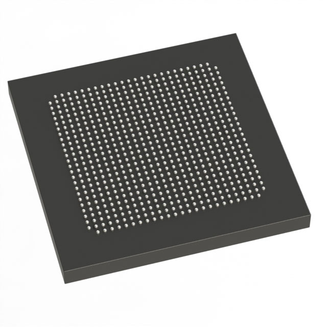
Stratix® IV GX Field Programmable Gate Array (FPGA) IC 372 17544192 228000 780-BBGA, FCBGA |
|---|---|
| Quantity | 72 Available (as of June 10, 2026) |

| Product Category | Field Programmable Gate Array (FPGA) |
|---|---|
| Manufacturer | Intel |
| Manufacturing Status | Obsolete |
| Manufacturer Standard Lead Time | Contact Us |
| Datasheet |
Specifications & Environmental
| Device Package | 780-FBGA (29x29) | Grade | Commercial | Operating Temperature | 0°C – 85°C | ||
|---|---|---|---|---|---|---|---|
| Package / Case | 780-BBGA, FCBGA | Number of I/O | 372 | Voltage | 870 mV - 930 mV | ||
| Mounting Method | Surface Mount | RoHS Compliance | RoHS Compliant | REACH Compliance | REACH Unknown | ||
| Moisture Sensitivity Level | 3 (168 Hours) | Number of LABs/CLBs | 9120 | Number of Logic Elements/Cells | 228000 | ||
| Number of Gates | N/A | ECCN | 3A001A7A | HTS Code | 8542.39.0001 | ||
| Qualification | N/A | Total RAM Bits | 17544192 |
Overview of EP4SGX230DF29C3N – Stratix® IV GX Field Programmable Gate Array (FPGA), 228000 logic elements
The EP4SGX230DF29C3N is an Intel Stratix IV GX FPGA featuring a high-capacity fabric and architecture elements targeted at high-throughput, protocol-rich designs. This device combines 228,000 logic elements with substantial on‑chip RAM and a large I/O complement to support complex system integration.
Documented as part of the Stratix IV family, the device handbook highlights core FPGA fabric features such as high-speed transceiver support, embedded memory, DSP blocks, clock networks and PLLs—making this part suitable for designs that require high aggregate data bandwidth and extensive I/O integration.
Key Features
- Logic Capacity Provides 228,000 logic elements for implementing large-scale digital designs and complex algorithms.
- Embedded Memory Approximately 17.5 Mbits of on-chip RAM (17,544,192 total RAM bits) to support buffering, lookup tables and local storage.
- I/O Density 372 I/O pins enable broad interfacing options for external peripherals, memory and high-density board designs.
- Stratix IV GX Architecture Device handbook entries describe Stratix IV GX family features including high-speed transceiver capabilities and wide protocol support.
- DSP and Timing Resources The device family documentation lists digital signal processing (DSP) blocks, clock networks and PLLs to support deterministic timing and signal-processing workloads.
- Power Supply Core supply specified between 870 mV and 930 mV, enabling designers to plan for the device’s core voltage requirements.
- Package & Mounting 780‑FBGA (29×29) surface‑mount package (listed as 780‑BBGA, FCBGA) for compact board-level integration.
- Operating Range Commercial grade operation from 0 °C to 85 °C.
- Regulatory RoHS‑compliant.
Typical Applications
- High‑bandwidth communications Where high aggregate data bandwidth and protocol support are required, the Stratix IV GX architecture and transceiver features provide the necessary foundation.
- Signal processing and DSP Large logic capacity and documented DSP block support make the device suitable for compute‑intensive signal-processing pipelines.
- High‑pin count system integration With 372 I/Os and an FCBGA package, the device supports dense external memory and peripheral interfaces on compact PCBs.
- External memory interfaces The device family explicitly addresses external memory interface support, useful for designs requiring extended buffering or high-throughput memory access.
Unique Advantages
- High logic density: 228,000 logic elements enable large designs or multiple concurrent functions on a single device.
- Significant on‑chip RAM: Approximately 17.5 Mbits of embedded memory reduces dependence on external RAM for many buffering and storage needs.
- Large I/O complement: 372 I/Os support complex board-level connectivity and multiple peripheral interfaces without external multiplexing.
- Family features documented in device handbook: Stratix IV GX family details include high-speed transceivers, DSP blocks, PLLs and clock networks—providing design resources for high-performance systems.
- Compact surface‑mount package: 780‑FBGA (29×29) package offers a high I/O density footprint for space-constrained applications.
- Commercial operating range and RoHS compliance: Supports standard commercial temperature operation (0 °C to 85 °C) and meets RoHS requirements for environmental compliance.
Why Choose EP4SGX230DF29C3N?
The EP4SGX230DF29C3N positions itself for projects that require substantial logic resources, sizeable embedded memory and a high number of I/Os in a compact FCBGA package. Backed by the Stratix IV GX device family documentation, the part provides architectural building blocks—such as transceiver support, DSP resources and robust clocking—that engineers can leverage for high-throughput, protocol-rich systems.
This device is well suited to design teams building complex communications, signal-processing or high-integration systems who need a commercially graded FPGA with verifiable specifications for core voltage, operating temperature and on-chip resource counts.
Request a quote or submit an inquiry to receive pricing and availability for EP4SGX230DF29C3N.


Date Founded: 1968
Headquarters: Santa Clara, California, USA
Employees: 130,000+
Revenue: $54.23 Billion
Certifications and Memberships: ISO9001:2015, ISO14001:2015, ISO17025:2017, ISO27001:2022, ISO45001:2018, ISO50001:2018


