
EPF10K130EFC484-2N
| Part Description |
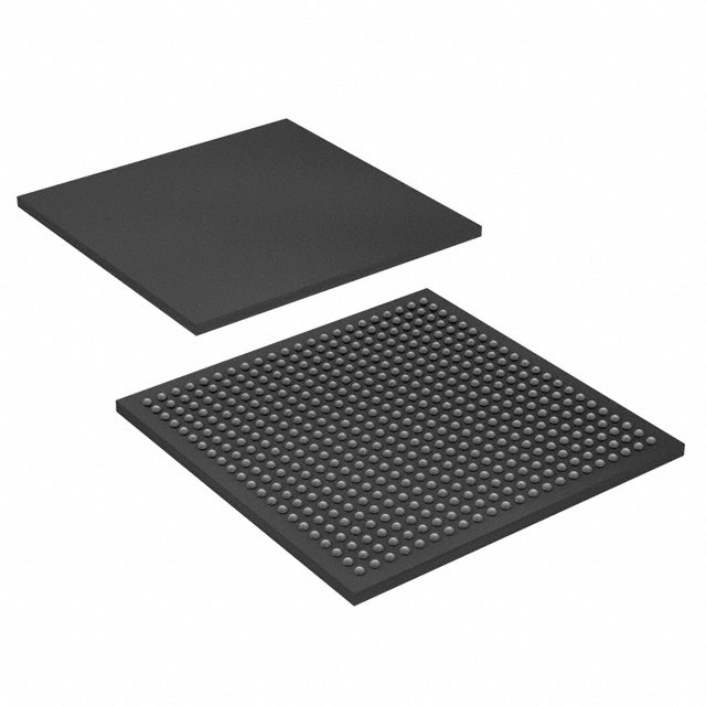
FLEX-10KE® Field Programmable Gate Array (FPGA) IC 369 65536 6656 484-BBGA |
|---|---|
| Quantity | 480 Available (as of June 18, 2026) |

| Product Category | Field Programmable Gate Array (FPGA) |
|---|---|
| Manufacturer | Intel |
| Manufacturing Status | Obsolete |
| Manufacturer Standard Lead Time | Contact Us |
| Datasheet |
Specifications & Environmental
| Device Package | 484-FBGA (23x23) | Grade | Commercial | Operating Temperature | 0°C – 70°C | ||
|---|---|---|---|---|---|---|---|
| Package / Case | 484-BBGA | Number of I/O | 369 | Voltage | 2.375 V - 2.625 V | ||
| Mounting Method | Surface Mount | RoHS Compliance | Unknown | REACH Compliance | REACH Unaffected | ||
| Moisture Sensitivity Level | 3 (168 Hours) | Number of LABs/CLBs | 832 | Number of Logic Elements/Cells | 6656 | ||
| Number of Gates | 342000 | ECCN | 3A001A2A | HTS Code | 8542.39.0001 | ||
| Qualification | N/A | Total RAM Bits | 65536 |
Overview of EPF10K130EFC484-2N – FLEX-10KE FPGA, 484-BBGA
The EPF10K130EFC484-2N is a FLEX-10KE field programmable gate array (FPGA) IC designed for mid-range programmable-logic integration. The device combines a logic array and embedded memory resources to implement megafunctions and general-purpose logic within a single, reconfigurable device.
This commercial-grade, RoHS-compliant device offers a balance of logic capacity, embedded RAM, and I/O density for system-level applications that require in-system reconfigurability, boundary-scan test access, and compact BGA packaging.
Key Features
- Core architecture Embedded array for implementing megafunctions and a separate logic array for general logic functions, enabling System-on-a-Programmable-Chip (SOPC) integration as described for the FLEX 10K family.
- Logic capacity Approximately 6,656 logic elements implemented across 832 LABs, providing substantial programmable logic resources.
- Embedded memory Total on-chip RAM of 65,536 bits for data buffering, state storage, and memory-based functions.
- I/O density and flexibility 369 user I/O pins with series I/O capabilities described in the FLEX 10K family, including individual tri-state control, open-drain options, and programmable output slew-rate control.
- System and test features Built-in JTAG boundary-scan test (BST) compliant with IEEE Std. 1149.1 for board-level test and in-circuit reconfigurability.
- Power and supply Operates from a supply range of 2.375 V to 2.625 V.
- Package and mounting 484-ball BGA package (484-BBGA; supplier package 484-FBGA 23×23) for surface-mount assembly and high board-area efficiency.
- Operating environment Commercial temperature grade with an operating range of 0 °C to 70 °C; RoHS compliant.
Typical Applications
- System integration and SOPC implementations Use the embedded array and logic fabric to consolidate custom peripherals, glue logic, and megafunctions into a programmable system block.
- Memory-backed logic functions Implement buffers, FIFOs, or small embedded-data stores using the device’s 65,536 bits of on-chip RAM.
- I/O consolidation and protocol bridging Leverage 369 I/Os and programmable I/O features to combine multiple interface signals or create custom protocol adapters.
- Board-level test and reconfiguration Use built-in JTAG boundary-scan for production test and to support in-circuit reconfiguration workflows.
Unique Advantages
- High programmable logic density: 6,656 logic elements across 832 LABs provide the resources needed for complex glue logic and mid-range FPGA functions.
- Substantial embedded memory: 65,536 bits of on-chip RAM reduce the need for external memory in many buffering and lookup applications.
- Large I/O count with flexible options: 369 user I/Os and programmable output features enable dense I/O mapping and signal-conditioning choices on a per-pin basis.
- Compact BGA packaging: 484-ball BGA (484-FBGA 23×23) delivers high pin count in a space-efficient surface-mount form factor.
- Built-in test and reconfiguration: IEEE-1149.1 JTAG boundary-scan support and in-circuit reconfigurability simplify board debug, programming, and production test.
- RoHS-compliant commercial solution: Commercial operating range and RoHS compliance help meet common regulatory and assembly requirements.
Why Choose EPF10K130EFC484-2N?
The EPF10K130EFC484-2N positions itself as a flexible, reconfigurable building block for designs that need a combination of logic density, embedded memory, and substantial I/O capacity in a compact BGA package. Its support for in-system reconfiguration and JTAG boundary-scan makes it suitable for development, prototyping, and production applications where board-level testability and configurability matter.
This device is well suited to engineers building mid-range programmable logic solutions who require a commercially graded, RoHS-compliant FPGA with defined supply and temperature limits, and who value the integration of embedded memory and extensive I/O in a single component.
Request a quote or submit an inquiry for pricing and availability of EPF10K130EFC484-2N.


Date Founded: 1968
Headquarters: Santa Clara, California, USA
Employees: 130,000+
Revenue: $54.23 Billion
Certifications and Memberships: ISO9001:2015, ISO14001:2015, ISO17025:2017, ISO27001:2022, ISO45001:2018, ISO50001:2018


