
EPF10K200SFC484-3N
| Part Description |
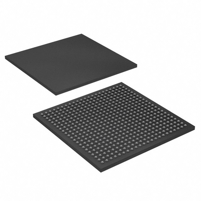
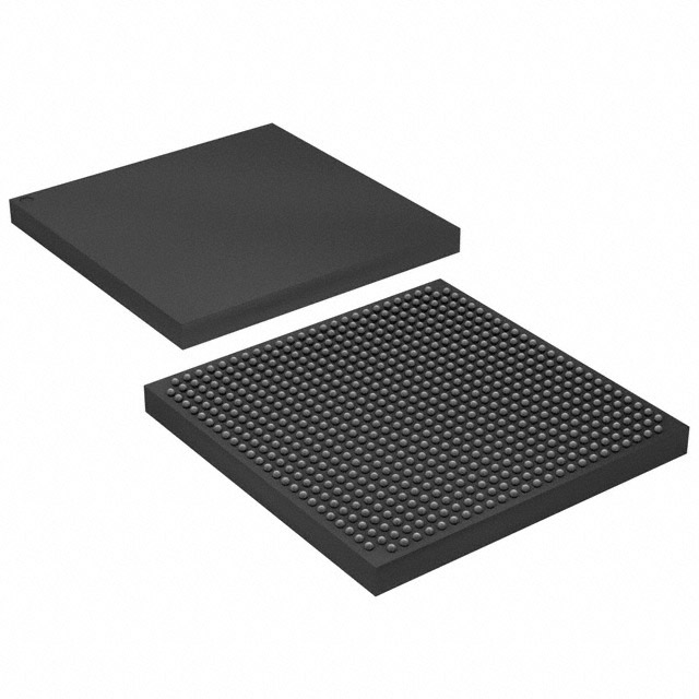
FLEX-10KS® Field Programmable Gate Array (FPGA) IC 369 98304 9984 484-BBGA |
|---|---|
| Quantity | 767 Available (as of June 15, 2026) |
| Product Category | Field Programmable Gate Array (FPGA) |
|---|---|
| Manufacturer | Intel |
| Manufacturing Status | Obsolete |
| Manufacturer Standard Lead Time | Contact Us |
| Datasheet |
Specifications & Environmental
| Device Package | 484-FBGA (23x23) | Grade | Commercial | Operating Temperature | 0°C – 70°C | ||
|---|---|---|---|---|---|---|---|
| Package / Case | 484-BBGA | Number of I/O | 369 | Voltage | 2.375 V - 2.625 V | ||
| Mounting Method | Surface Mount | RoHS Compliance | Unknown | REACH Compliance | REACH Unaffected | ||
| Moisture Sensitivity Level | 3 (168 Hours) | Number of LABs/CLBs | 1248 | Number of Logic Elements/Cells | 9984 | ||
| Number of Gates | 513000 | ECCN | 3A001A2A | HTS Code | 8542.39.0001 | ||
| Qualification | N/A | Total RAM Bits | 98304 |
Overview of EPF10K200SFC484-3N – FLEX-10KS Field Programmable Gate Array, 484-BBGA
The EPF10K200SFC484-3N is a FLEX 10K family field programmable gate array (FPGA) in a compact 484-ball BGA package. It combines a high density of logic elements with substantial on-chip memory and a large I/O count to support system-level integration and programmable logic functions.
Designed for commercial-grade applications, this device provides embedded memory, in-circuit reconfigurability via JTAG/configuration devices, and a broad I/O complement for complex digital designs where integration and board-space efficiency matter.
Key Features
- Logic Capacity — 9,984 logic elements providing the programmable fabric for combinational and sequential logic.
- Embedded Memory — Approximately 98 kbits (98,304 bits) of on-chip RAM to support buffers, FIFOs, and small data tables without external memory.
- I/O Density — 369 user I/O pins to interface with multiple peripherals, sensors, and high-pin-count subsystems.
- Gate Count — 513,000 gates for mapping larger logic functions and system glue logic.
- Logic Array Blocks (LABs) — 1,248 LABs for structured logic partitioning and efficient place-and-route.
- In-Circuit Reconfigurability & JTAG — Supports in-circuit reconfiguration and includes JTAG boundary-scan for device programming and board-level testability.
- Package & Mounting — 484-BBGA package; supplier device package listed as 484-FBGA (23×23). Surface-mount mounting type for modern PCB assembly.
- Power — Core/operating supply range of 2.375 V to 2.625 V to match target system power domains.
- Operating Temperature — Commercial grade operation from 0 °C to 70 °C.
- Environmental Compliance — RoHS compliant for lead-free assembly and regulatory support.
Typical Applications
- System-on-a-Programmable-Chip (SOPC) — Integration of custom logic, on-chip memory, and high-density I/O for compact system-level designs.
- Prototyping and Development — Reconfigurable logic and JTAG support make the device suitable for iterative design and validation of digital subsystems.
- High-I/O Signal Glue and Interface Bridging — Large I/O count enables use as an interface bridge or glue logic between multiple peripherals and controllers.
- Embedded Control and Logic Acceleration — On-chip RAM and substantial logic resources support control tasks, state machines, and accelerators within commercial electronic products.
Unique Advantages
- High Logic Integration: Nearly 10,000 logic elements and 513,000 gates allow substantial integration of digital functions into a single device, reducing BOM count.
- On-Chip Memory: Approximately 98 kbits of embedded RAM supports local buffering and small data structures without external memory components.
- Extensive I/O: 369 user I/O pins provide flexibility for multi-channel interfaces, sensor arrays, and peripheral connections.
- Compact, Surface-Mount BGA: 484-ball BGA packaging and surface-mount mounting enable dense board layouts and efficient use of PCB area.
- In-System Reconfiguration and Test: JTAG boundary-scan and in-circuit reconfigurability simplify programming, debug, and board-level test strategies.
- Regulatory Readiness: RoHS compliance supports modern assembly and regulatory needs for commercial products.
Why Choose EPF10K200SFC484-3N?
The EPF10K200SFC484-3N positions itself as a commercially graded, highly integrated FPGA option for designers who need a balance of logic capacity, embedded memory, and extensive I/O in a compact BGA package. Its combination of nearly 10,000 logic elements, substantial on-chip RAM, and 369 I/Os makes it suitable for mid-density programmable logic tasks and system integration where board space and flexibility are important.
For engineering teams building programmable control logic, interface bridging, or SOPC-style subsystems, this device delivers reconfigurability and testability (via JTAG) while meeting common commercial temperature and RoHS requirements—helping accelerate development and simplify BOMs.
Request a quote or submit a pricing inquiry to check availability and lead times for EPF10K200SFC484-3N. Our team can provide ordering information and assist with technical packaging or supply questions.


Date Founded: 1968
Headquarters: Santa Clara, California, USA
Employees: 130,000+
Revenue: $54.23 Billion
Certifications and Memberships: ISO9001:2015, ISO14001:2015, ISO17025:2017, ISO27001:2022, ISO45001:2018, ISO50001:2018


