
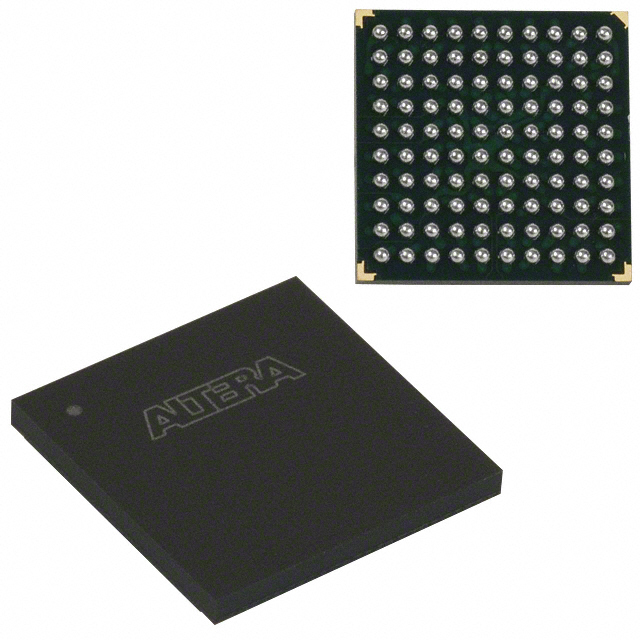
EPF6016AFC256-3
| Part Description |
FLEX 6000 Field Programmable Gate Array (FPGA) IC 171 1320 256-BGA |
|---|---|
| Quantity | 1,340 Available (as of June 16, 2026) |

| Product Category | Field Programmable Gate Array (FPGA) |
|---|---|
| Manufacturer | Intel |
| Manufacturing Status | Obsolete |
| Manufacturer Standard Lead Time | Contact Us |
| Datasheet |
Specifications & Environmental
| Device Package | 256-FBGA (17x17) | Grade | Commercial | Operating Temperature | 0°C – 85°C | ||
|---|---|---|---|---|---|---|---|
| Package / Case | 256-BGA | Number of I/O | 171 | Voltage | 3 V - 3.6 V | ||
| Mounting Method | Surface Mount | RoHS Compliance | Unknown | REACH Compliance | REACH Unaffected | ||
| Moisture Sensitivity Level | 3 (168 Hours) | Number of LABs/CLBs | 132 | Number of Logic Elements/Cells | 1320 | ||
| Number of Gates | 16000 | ECCN | 3A001A2A | HTS Code | 8542.39.0001 | ||
| Qualification | N/A |
Overview of EPF6016AFC256-3 – FLEX 6000 Field Programmable Gate Array (FPGA), 1,320 Logic Elements, 171 I/O, 256‑BGA
The EPF6016AFC256-3 is a member of the FLEX 6000 programmable logic family offering a register-rich, LUT-based OptiFLEX architecture for reprogrammable, application-specific logic in commercial designs. With 1,320 logic elements and an equivalent of 16,000 typical gates, it targets prototyping, design testing, and custom control and interface functions where reconfigurability and high I/O count matter.
Packaged in a 256‑FBGA (17×17) surface-mount package and specified for a 3.0 V to 3.6 V supply and 0 °C to 85 °C operating range, the device integrates features for predictable timing, flexible I/O interfacing, and system-level testability.
Key Features
- Core Architecture Register-rich, look-up table (LUT) based OptiFLEX architecture providing 1,320 logic elements and approximately 16,000 typical gates for implementing custom digital logic.
- I/O and Interface Up to 171 I/O pins with MultiVolt™ I/O interface capability to bridge between different voltage domains and individual tri-state output enable control per pin.
- Interconnect and Arithmetic Support FastTrack® continuous routing structure, dedicated carry chain for fast arithmetic (adders, counters) and dedicated cascade chain for high‑fan‑in logic functions.
- Clocking and Timing Built-in low-skew clock distribution tree and four low-skew global paths to support clock, clear, preset, or logic signals for predictable timing.
- System-Level Reconfiguration & Test Reprogrammable SRAM elements with support for in-circuit reconfigurability via external configuration device or intelligent controller; integrated IEEE Std. 1149.1 JTAG boundary-scan test circuitry.
- Package & Mounting 256‑FBGA (17×17) fine-pitch BGA package, surface-mountable, suited for compact board-level designs requiring higher pin density.
- Electrical & Environmental Voltage supply range of 3.0 V to 3.6 V, commercial operating temperature range of 0 °C to 85 °C, and RoHS compliant.
Typical Applications
- Prototyping and Design Validation Reprogrammable architecture and in-circuit reconfigurability make the device suitable for rapid iteration and functional testing of custom logic prior to production.
- Interface Bridging and Glue Logic MultiVolt I/O and 171 available I/O pins enable protocol translation, domain bridging, and integration of diverse peripherals in commercial systems.
- Control and Sequencing Use the dedicated carry and cascade chains for efficient implementation of adders, counters, and high‑fan‑in control logic in embedded controllers and user interfaces.
- Board-Level Test and Debug Built-in IEEE 1149.1 JTAG boundary-scan provides on-board testability and simplifies system bring-up and diagnostics.
Unique Advantages
- Flexible, reprogrammable platform: Reconfigurable SRAM-based device enables design changes in-circuit and rapid prototyping without respins of fixed silicon.
- High I/O density in a compact package: 171 I/O in a 256‑FBGA (17×17) package reduces board-level routing complexity while supporting many external interfaces.
- Predictable interconnect and timing: FastTrack interconnect and low-skew clock distribution improve timing predictability for synchronous designs.
- Optimized arithmetic and logic primitives: Dedicated carry and cascade chains accelerate implementation of adders, counters, and high‑fan‑in logic, reducing resource consumption.
- System testability and reconfiguration: Integrated IEEE 1149.1 JTAG and support for in-circuit reconfiguration simplify debugging, upgrades, and field maintenance.
- Commercial-grade supply and compliance: 3.0–3.6 V supply range, 0 °C–85 °C operating range, and RoHS compliance for broad commercial applications.
Why Choose EPF6016AFC256-3?
The EPF6016AFC256-3 provides a balanced combination of reprogrammable logic capacity, extensive I/O, and proven FLEX 6000 family architecture suited to commercial embedded designs, prototyping, and interface-rich applications. Its OptiFLEX architecture and dedicated arithmetic/cascade resources let engineers implement complex control and glue logic with predictable routing and timing.
This device is an appropriate choice for teams seeking a reconfigurable, board-friendly FPGA in a 256‑FBGA package with integrated testability and broad software design support across the FLEX 6000 family for scalable design migration and footprint compatibility.
Request a quote or submit a pricing inquiry to check availability and delivery for the EPF6016AFC256-3.


Date Founded: 1968
Headquarters: Santa Clara, California, USA
Employees: 130,000+
Revenue: $54.23 Billion
Certifications and Memberships: ISO9001:2015, ISO14001:2015, ISO17025:2017, ISO27001:2022, ISO45001:2018, ISO50001:2018


