
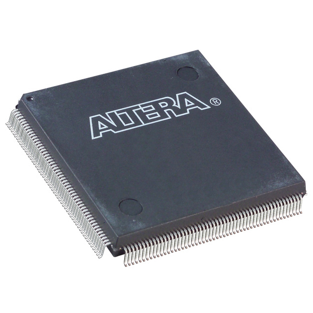
EPF6016AQC208-1
| Part Description |
FLEX 6000 Field Programmable Gate Array (FPGA) IC 171 1320 208-BFQFP |
|---|---|
| Quantity | 1,471 Available (as of June 18, 2026) |
| Product Category | Field Programmable Gate Array (FPGA) |
|---|---|
| Manufacturer | Intel |
| Manufacturing Status | Obsolete |
| Manufacturer Standard Lead Time | Contact Us |
| Datasheet |
Specifications & Environmental
| Device Package | 208-PQFP (28x28) | Grade | Commercial | Operating Temperature | 0°C – 85°C | ||
|---|---|---|---|---|---|---|---|
| Package / Case | 208-BFQFP | Number of I/O | 171 | Voltage | 3 V - 3.6 V | ||
| Mounting Method | Surface Mount | RoHS Compliance | RoHS non-compliant | REACH Compliance | REACH Unaffected | ||
| Moisture Sensitivity Level | 3 (168 Hours) | Number of LABs/CLBs | 132 | Number of Logic Elements/Cells | 1320 | ||
| Number of Gates | 16000 | ECCN | 3A991D | HTS Code | 8542.39.0001 | ||
| Qualification | N/A |
Overview of EPF6016AQC208-1 – FLEX 6000 FPGA, 1,320 logic elements, 171 I/O, 208-BFQFP
The EPF6016AQC208-1 is a FLEX 6000 family field-programmable gate array (FPGA) from Intel. Based on the OptiFLEX architecture and a register‑rich, LUT‑based structure, this device targets low‑cost programmable logic applications where in‑system reconfigurability and fast design change are important.
With 1,320 logic elements, approximately 16,000 typical gates, 171 I/O pins and a 208‑pin PQFP package, the device is suited for prototyping, control and interface functions in commercial‑grade systems that operate from 3.0 V to 3.6 V and across 0 °C to 85 °C.
Key Features
- OptiFLEX architecture & LUT-based core Register‑rich look‑up table (LUT) architecture optimized for area efficiency and flexible logic implementation.
- 1,320 logic elements / ~16,000 typical gates Device density that supports medium‑complexity logic and control functions within a compact package footprint.
- Reconfigurable SRAM elements On‑device reprogrammability enables rapid prototyping and in‑circuit design updates.
- Power and supply Operates from 3.0 V to 3.6 V, with low standby current characteristics described for the FLEX 6000 family.
- Robust I/O 171 I/O pins with individual tri‑state output enable control and programmable output slew‑rate to manage switching noise and interface timing.
- Clock and routing Built‑in low‑skew clock distribution and dedicated fast paths (carry and cascade chains) for arithmetic and high‑fan‑in logic functions.
- In‑circuit reconfigurability & JTAG Supports in‑circuit reconfiguration via external configuration devices or controllers and includes IEEE 1149.1 JTAG boundary‑scan test circuitry without consuming device logic.
- Package & mounting Surface‑mount 208‑pin PQFP (208‑BFQFP) package (supplier device package: 208‑PQFP, 28×28) for standard PCB assembly.
- Commercial temperature and RoHS Rated for 0 °C to 85 °C operating temperature and RoHS compliant.
Typical Applications
- Prototyping and design validation In‑system reprogrammability and SRAM‑based configuration make this device suitable for iterative hardware development and design testing.
- Interface bridging and protocol glue logic Multi‑I/O capability and programmable slew control support bridging between different digital subsystems and custom interface logic.
- Embedded control and state machines The register‑rich architecture and dedicated arithmetic chains simplify implementation of control logic, counters, and comparators.
- Consumer and commercial electronics Medium‑density programmable logic for user interfaces, peripheral control, and system glue in commercial‑grade products.
Unique Advantages
- Flexible reprogrammability: Reconfigurable SRAM elements enable rapid design changes and in‑circuit updates without hardware swaps.
- Balanced density and I/O: 1,320 logic elements combined with 171 I/O pins provide a practical mix of logic capacity and external connectivity for mid‑range designs.
- Deterministic clocking and fast paths: Low‑skew clock distribution plus dedicated carry and cascade chains reduce design complexity for arithmetic and timing‑critical functions.
- Built‑in test support: IEEE 1149.1 JTAG boundary‑scan is available without consuming user logic, simplifying board‑level test and debug.
- Package compatibility: 208‑pin PQFP surface‑mount package fits standard PCB workflows while offering significant I/O density.
- Regulatory and commercial readiness: RoHS compliance and commercial temperature rating make the device suitable for mainstream product lines and procurement.
Why Choose EPF6016AQC208-1?
The EPF6016AQC208-1 offers a practical combination of programmable logic capacity, extensive I/O, and family‑level features such as OptiFLEX architecture, built‑in JTAG, and in‑circuit reconfigurability. Its medium density and 208‑pin PQFP package make it appropriate for designers seeking a cost‑effective, reprogrammable alternative to fixed gate arrays for commercial‑grade products.
This device is well suited to teams focused on rapid prototyping, interface logic consolidation and embedded control where the ability to iterate designs and perform board‑level testing without consuming user logic is valuable. Supported supply and temperature ranges align with standard commercial system requirements.
Request a quote or submit an inquiry to receive pricing and availability information for the EPF6016AQC208-1. Our team can provide lead‑time and sourcing details to support your design schedule.


Date Founded: 1968
Headquarters: Santa Clara, California, USA
Employees: 130,000+
Revenue: $54.23 Billion
Certifications and Memberships: ISO9001:2015, ISO14001:2015, ISO17025:2017, ISO27001:2022, ISO45001:2018, ISO50001:2018


