
EPF6016BC256-2
| Part Description |
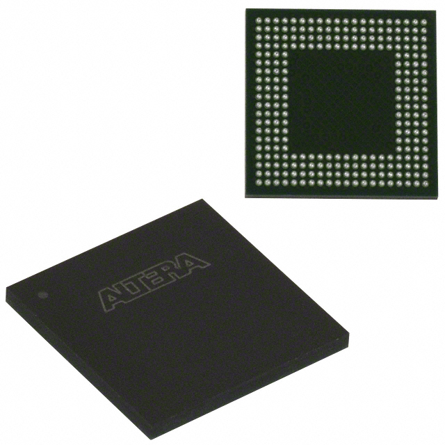
FLEX 6000 Field Programmable Gate Array (FPGA) IC 204 1320 256-LBGA |
|---|---|
| Quantity | 971 Available (as of June 15, 2026) |

| Product Category | Field Programmable Gate Array (FPGA) |
|---|---|
| Manufacturer | Intel |
| Manufacturing Status | Obsolete |
| Manufacturer Standard Lead Time | Contact Us |
| Datasheet |
Specifications & Environmental
| Device Package | 256-BGA (27x27) | Grade | Commercial | Operating Temperature | 0°C – 85°C | ||
|---|---|---|---|---|---|---|---|
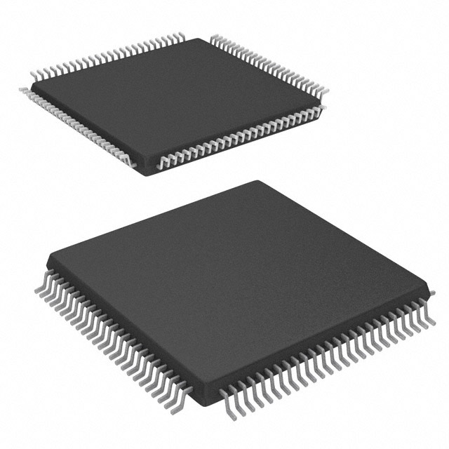
| Package / Case | 256-LBGA | Number of I/O | 204 | Voltage | 4.75 V - 5.25 V | ||
| Mounting Method | Surface Mount | RoHS Compliance | RoHS non-compliant | REACH Compliance | REACH Unaffected | ||
| Moisture Sensitivity Level | 3 (168 Hours) | Number of LABs/CLBs | 132 | Number of Logic Elements/Cells | 1320 | ||
| Number of Gates | 16000 | ECCN | 3A991D | HTS Code | 8542.39.0001 | ||
| Qualification | N/A |
Overview of EPF6016BC256-2 – FLEX 6000 Field Programmable Gate Array (FPGA) IC 204 1320 256-LBGA
The EPF6016BC256-2 is a FLEX 6000 family programmable logic device offering a register-rich, LUT-based architecture with OptiFLEX area optimization and reconfigurable SRAM elements. This 5.0-V device provides 1,320 logic elements, approximately 16,000 typical gates, and up to 204 I/O in a 256-ball BGA (27 × 27 mm) package for surface-mount applications.
Engineered for low-cost gate-array replacement, rapid prototyping, and in-system reconfiguration, the device supports system-level features such as in-circuit reconfiguration and IEEE 1149.1 JTAG boundary-scan. Its commercial-grade operating range and RoHS compliance make it suitable for a wide range of standard embedded and interface-control designs.
Key Features
- Core Architecture
Register-rich, LUT-based OptiFLEX architecture with dedicated carry and cascade chains to support fast arithmetic and high‑fan‑in logic functions. - Logic Resources
1,320 logic elements and approximately 16,000 typical gates for medium-density programmable logic implementations. - I/O and Interface
Up to 204 I/O pins with individual tri-state output enable and programmable output slew-rate control for signal integrity and flexible interfacing. - Configuration and Test
In-circuit reconfigurability via external configuration device or intelligent controller, plus built-in IEEE 1149.1 JTAG boundary-scan for board-level test without consuming user logic. - Clocking and Interconnect
Built-in low-skew clock distribution tree and FastTrack continuous routing structure for predictable timing; dedicated carry and cascade chains accelerate arithmetic and complex logic. - Power and Voltage
5.0-V device with supply range 4.75 V to 5.25 V and low-power standby behavior noted in the family data. - Package and Mounting
256-LBGA (256-ball BGA, 27 × 27 mm) surface-mount package for dense board layouts and reliable soldered connections. - Operating Range and Compliance
Commercial operating temperature 0 °C to 85 °C and RoHS compliance for regulatory and environmental considerations.
Typical Applications
- Prototyping and Development
Rapid design iteration and functional testing where in-circuit reconfigurability and reprogrammable logic reduce development cycles. - Gate-Array Replacement
Cost-sensitive designs that require a programmable alternative to fixed gate-array implementations while preserving gate-count parity. - Interface and Glue Logic
Custom bus bridging, signal conditioning, and peripheral interfacing using the device’s 204 I/O pins and programmable I/O controls. - Board-Level Test and Validation
Built-in JTAG boundary-scan simplifies board test and debug without consuming additional user logic resources.
Unique Advantages
- Reprogrammable Flexibility:
In-circuit reconfiguration enables field updates and design changes without board replacement, reducing lifecycle cost. - Medium-Density Integration:
1,320 logic elements and ~16,000 gates provide a balance of capacity and cost for many embedded logic functions. - Robust I/O Capability:
204 configurable I/O pins with individual output enable and slew-rate control help manage signal integrity across mixed-voltage systems. - Test-Ready Design:
IEEE 1149.1 JTAG boundary-scan is available without consuming device logic, streamlining manufacturing test and board-level diagnostics. - Package Density:
256-ball BGA (27 × 27 mm) delivers high pin count in a compact surface-mount footprint for space-constrained boards. - Proven Family Features:
OptiFLEX architecture, low-skew clocking, and dedicated arithmetic chains provide predictable routing and performance for deterministic designs.
Why Choose EPF6016BC256-2?
The EPF6016BC256-2 combines the FLEX 6000 family’s OptiFLEX architecture and reconfigurable SRAM-based logic to deliver a practical, programmable alternative to fixed gate-array solutions. With 1,320 logic elements, roughly 16,000 gates, extensive I/O and built-in test/configuration features, it is well suited for engineers needing medium-density programmable logic with in-system flexibility.
This device is aimed at teams developing prototypes, custom interface logic, and designs that benefit from field reconfiguration, board-level boundary-scan, and cost-effective integration in a 256-BGA surface-mount package. Its commercial temperature range and RoHS compliance support deployment across standard embedded applications.
Request a quote or submit an inquiry for pricing and availability of EPF6016BC256-2 to begin your design evaluation and procurement process.


Date Founded: 1968
Headquarters: Santa Clara, California, USA
Employees: 130,000+
Revenue: $54.23 Billion
Certifications and Memberships: ISO9001:2015, ISO14001:2015, ISO17025:2017, ISO27001:2022, ISO45001:2018, ISO50001:2018


