
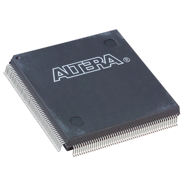
EPF6016QC208-2
| Part Description |
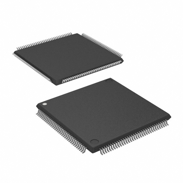
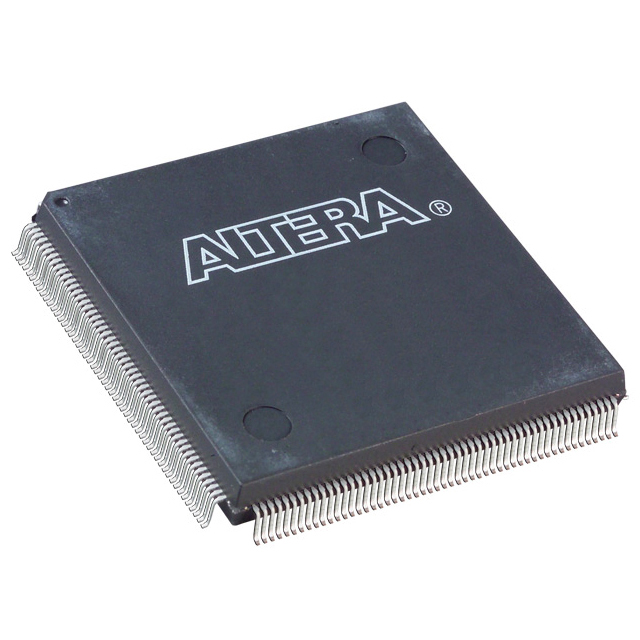
FLEX 6000 Field Programmable Gate Array (FPGA) IC 171 1320 208-BFQFP |
|---|---|
| Quantity | 482 Available (as of October 8, 2026) |
| Product Category | Field Programmable Gate Array (FPGA) |
|---|---|
| Manufacturer | Intel |
| Manufacturing Status | Obsolete |
| Manufacturer Standard Lead Time | Contact Us |
| Datasheet |
Specifications & Environmental
| Device Package | 208-PQFP (28x28) | Grade | Commercial | Operating Temperature | 0°C – 85°C | ||
|---|---|---|---|---|---|---|---|
| Package / Case | 208-BFQFP | Number of I/O | 171 | Voltage | 4.75 V - 5.25 V | ||
| Mounting Method | Surface Mount | RoHS Compliance | RoHS non-compliant | REACH Compliance | REACH Unaffected | ||
| Moisture Sensitivity Level | 6 (Time on Label) | Number of LABs/CLBs | 132 | Number of Logic Elements/Cells | 1320 | ||
| Number of Gates | 16000 | ECCN | 3A991D | HTS Code | 8542.39.0001 | ||
| Qualification | N/A |
Overview of EPF6016QC208-2 – FLEX 6000 Field Programmable Gate Array (FPGA) IC 171 I/O 1320 Logic Elements 208-BFQFP
The EPF6016QC208-2 is a FLEX 6000 family field programmable gate array (FPGA) from Intel (Altera). It is based on the OptiFLEX architecture and provides a reprogrammable, register-rich, LUT-based logic fabric intended as a low-cost, programmable alternative to fixed gate-array designs.
Key hardware specifics for this device include 1,320 logic elements, approximately 16,000 typical gates, 171 I/O pins in a 208-pin fine-pitch quad flat package, a 5.0 V nominal supply (4.75 V to 5.25 V), and a commercial operating temperature range of 0 °C to 85 °C.
Key Features
- Core Architecture — OptiFLEX, register-rich LUT-based architecture delivering 1,320 logic elements and approximately 16,000 typical gates for flexible logic implementation.
- I/O and Interface — 171 user I/O pins with individual tri-state output-enable control and programmable output slew-rate control; supports MultiVolt I/O interface operation to bridge between systems at different voltages.
- Configuration & Test — In-circuit reconfigurability (ICR) via external configuration device or intelligent controller and built-in IEEE Std. 1149.1 JTAG boundary-scan test circuitry available without consuming user logic.
- Dedicated Arithmetic Support — Dedicated carry and cascade chains for efficient implementation of adders, counters, comparators, and high-fan-in logic functions.
- Interconnect & Clocking — FastTrack continuous routing structure for predictable interconnect delays and a built-in low-skew clock distribution tree with four low-skew global paths for clock/clear/preset or logic signals.
- Power & Standby — 5.0 V device operation with a supply range of 4.75 V to 5.25 V; family-level standby behavior includes low power consumption characteristics.
- Package & Mounting — Surface-mount 208-BFQFP package (supplier package: 208-PQFP 28×28) suitable for compact PCB designs; RoHS compliant.
- Grade & Environment — Commercial grade device rated for 0 °C to 85 °C operation and RoHS compliant.
- On-Chip Memory — No embedded on-chip RAM (total RAM bits: 0) for designs that rely solely on logic resources and external memory.
Typical Applications
- Prototyping & Design Validation — Rapidly iterate hardware designs and test gate-array replacements using the device’s reprogrammable logic and in-circuit reconfiguration capabilities.
- Low-Cost Gate-Array Replacement — Implement medium-density logic functions as a programmable alternative to custom gate arrays, reducing NRE and enabling late-stage design changes.
- System Glue Logic & Interface Bridging — Use the device’s MultiVolt I/O and abundant I/O pins to bridge components operating at different voltages and consolidate glue logic into a single programmable device.
- Boundary-Scan Testability — Integrate JTAG boundary-scan for board-level testing and manufacturing diagnostics without consuming user logic resources.
Unique Advantages
- Flexible, Reprogrammable Platform: OptiFLEX architecture and in-circuit reconfiguration let teams change functionality during prototyping or in-field updates without hardware redesign.
- Mid-Density Logic Capacity: 1,320 logic elements and ~16,000 gates provide sufficient density for medium-complexity logic implementations while keeping BOM costs predictable.
- Rich I/O Capability: 171 I/O pins with per-pin output enable and programmable slew rate simplify interface design and signal integrity tuning on mixed-voltage systems.
- Test and Manufacturing Support: Built-in IEEE 1149.1 JTAG boundary-scan enables board-level test and diagnostics without using the device’s logic resources.
- Package Flexibility: 208-pin fine-pitch quad flat package in a surface-mount form factor supports compact PCB layouts and common assembly flows.
- Standards Compatibility: As a 5.0 V device, the family supports compliance with the PCI Local Bus Specification, Revision 2.2, where applicable.
Why Choose EPF6016QC208-2?
The EPF6016QC208-2 positions itself as a commercially graded, mid-density FPGA option for engineers and procurement teams seeking a programmable alternative to gate-array implementations. With 1,320 logic elements, ~16,000 typical gates, and 171 I/O pins in a 208-pin surface-mount package, it targets applications that require flexible logic integration, robust I/O, and production-ready packaging.
This device is suited for design teams working on prototypes, system glue logic, or moderate-complexity digital functions that benefit from reprogrammability, boundary-scan testing, and MultiVolt interfacing. Its commercial temperature rating and RoHS compliance make it appropriate for a broad range of general-purpose electronic products and development projects.
Request a quote or submit an inquiry to receive availability and pricing information for the EPF6016QC208-2. Our team can provide lead-time details and support for procurement and integration planning.






















Date Founded: 1968
Headquarters: Santa Clara, California, USA
Employees: 130,000+
Revenue: $54.23 Billion
Certifications and Memberships: ISO9001:2015, ISO14001:2015, ISO17025:2017, ISO27001:2022, ISO45001:2018, ISO50001:2018


