
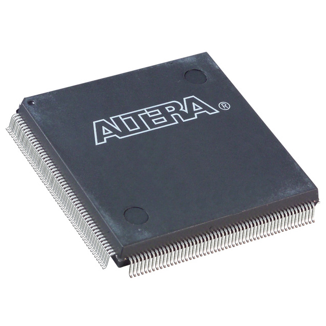
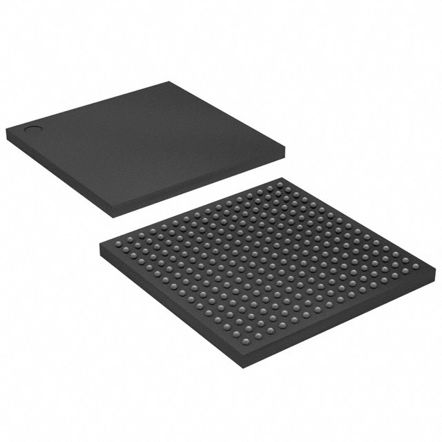
EPF6024AFC256-3
| Part Description |
FLEX 6000 Field Programmable Gate Array (FPGA) IC 219 1960 256-BGA |
|---|---|
| Quantity | 949 Available (as of June 16, 2026) |

| Product Category | Field Programmable Gate Array (FPGA) |
|---|---|
| Manufacturer | Intel |
| Manufacturing Status | Obsolete |
| Manufacturer Standard Lead Time | Contact Us |
| Datasheet |
Specifications & Environmental
| Device Package | 256-FBGA (17x17) | Grade | Commercial | Operating Temperature | 0°C – 85°C | ||
|---|---|---|---|---|---|---|---|
| Package / Case | 256-BGA | Number of I/O | 219 | Voltage | 3 V - 3.6 V | ||
| Mounting Method | Surface Mount | RoHS Compliance | Unknown | REACH Compliance | REACH Unaffected | ||
| Moisture Sensitivity Level | 3 (168 Hours) | Number of LABs/CLBs | 196 | Number of Logic Elements/Cells | 1960 | ||
| Number of Gates | 24000 | ECCN | 3A001A2A | HTS Code | 8542.39.0001 | ||
| Qualification | N/A |
Overview of EPF6024AFC256-3 – FLEX 6000 FPGA, 1,960 logic elements, 219 I/O, 256-FBGA
The EPF6024AFC256-3 is a member of the FLEX 6000 programmable logic device family. It implements a register-rich, LUT-based architecture (OptiFLEX) designed for low-cost, reprogrammable logic in prototyping, design testing, and low- to medium-density logic integration.
This device provides 1,960 logic elements (typical 24,000 gates), 219 I/O pins in a 256-FBGA (17×17) package, and supports in-circuit reconfigurability and standard boundary-scan testability for flexible system integration and board-level test strategies.
Key Features
- Logic Capacity — 1,960 logic elements (typical 24,000 gates) suitable for mid-density programmable logic functions.
- I/O and Interface — 219 I/O pins with individual tri-state output enable control and programmable output slew-rate to help manage signal integrity and mixed-voltage interfacing.
- Reconfigurability — In-circuit reconfigurability via external configuration device or intelligent controller for fast design iteration and field updates.
- Clocking and Timing — Built-in low-skew clock distribution tree and four low-skew global paths for clock, clear, preset, or logic signals to support synchronous designs.
- Dedicated Arithmetic and Logic Chains — Dedicated carry and cascade chains for implementing fast adders, counters, comparators, and high-fan-in logic functions.
- Test and Debug — Built-in JTAG boundary-scan (IEEE Std. 1149.1-1990) for board-level testing without consuming device logic; note that the embedded JTAG circuitry can add up to 14,000 gates in addition to listed typical gates.
- Flexible Interconnect — FastTrack continuous routing structure for predictable interconnect delays and efficient place-and-route.
- Package and Mounting — 256-FBGA (17×17) surface-mount package for compact board designs; commercial-grade device with RoHS compliance.
- Power and Environmental — Supply voltage 3.0 V to 3.6 V and commercial operating temperature range 0 °C to 85 °C.
Typical Applications
- Prototyping and Design Validation — Rapid device reprogramming supports iterative hardware development and functional testing during product bring-up.
- In-Circuit Reconfigurable Systems — In-circuit reconfigurability enables field updates and functional changes via external configuration devices or controllers.
- Mixed-Voltage Interfaces — MultiVolt I/O interface operation allows bridging between systems operating at different I/O voltages while using a 3.0–3.6 V supply for the device core.
- Arithmetic and Control Logic — Dedicated carry and cascade chains make the device suitable for implementing adders, counters, comparators, and other control logic functions.
Unique Advantages
- Reprogrammable Flexibility: Supports in-circuit reconfiguration to shorten development cycles and enable field updates without board changes.
- Balanced Logic Density: 1,960 logic elements and ~24,000 typical gates provide mid-range capacity for consolidating glue logic and control functions.
- Strong I/O Control: 219 I/O pins with individual tri-state enables and slew-rate control help optimize signal integrity across multiple interfaces.
- Built-in Testability: IEEE 1149.1 boundary-scan support simplifies board-level test and diagnostics without consuming core logic resources.
- Compact, Surface-Mount Package: 256-FBGA (17×17) package offers a compact footprint for space-constrained designs while maintaining a high pin count.
- Vendor Toolchain Support: The FLEX 6000 family is supported by vendor development and place-and-route tools to streamline design implementation and verification.
Why Choose EPF6024AFC256-3?
The EPF6024AFC256-3 positions itself as a flexible, mid-density FPGA option within the FLEX 6000 family, combining a register-rich LUT architecture with dedicated arithmetic chains and comprehensive I/O control. Its 256-FBGA package and 219 I/O pins make it suitable for compact designs that require moderate logic integration and board-level testability.
This device is well suited to teams needing rapid prototyping, in-field reconfiguration, and reliable boundary-scan testing, delivered in a commercial-grade, RoHS-compliant package with a 3.0–3.6 V supply range and 0 °C to 85 °C operating temperature.
Request a quote or submit a request for pricing and availability to evaluate EPF6024AFC256-3 for your next design.


Date Founded: 1968
Headquarters: Santa Clara, California, USA
Employees: 130,000+
Revenue: $54.23 Billion
Certifications and Memberships: ISO9001:2015, ISO14001:2015, ISO17025:2017, ISO27001:2022, ISO45001:2018, ISO50001:2018


