
EPF6024AFI256-2
| Part Description |
FLEX 6000 Field Programmable Gate Array (FPGA) IC 219 1960 256-BGA |
|---|---|
| Quantity | 796 Available (as of June 18, 2026) |
| Product Category | Field Programmable Gate Array (FPGA) |
|---|---|
| Manufacturer | Intel |
| Manufacturing Status | Obsolete |
| Manufacturer Standard Lead Time | Contact Us |
| Datasheet |
Specifications & Environmental
| Device Package | 256-FBGA (17x17) | Grade | Industrial | Operating Temperature | -40°C – 100°C | ||
|---|---|---|---|---|---|---|---|
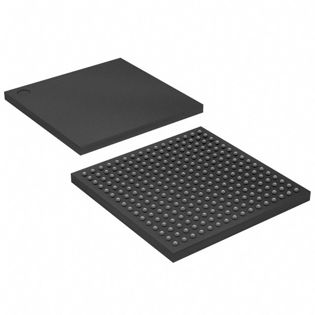
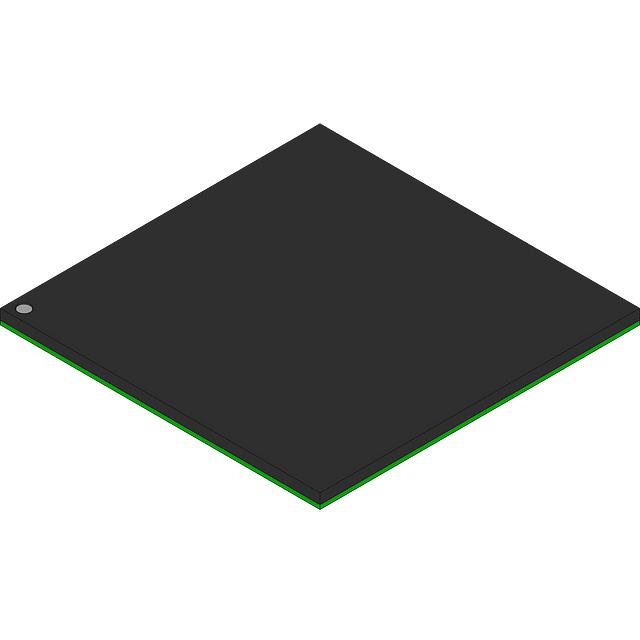
| Package / Case | 256-BGA | Number of I/O | 219 | Voltage | 3 V - 3.6 V | ||
| Mounting Method | Surface Mount | RoHS Compliance | RoHS non-compliant | REACH Compliance | REACH Unaffected | ||
| Moisture Sensitivity Level | 3 (168 Hours) | Number of LABs/CLBs | 196 | Number of Logic Elements/Cells | 1960 | ||
| Number of Gates | 24000 | ECCN | 3A991D | HTS Code | 8542.39.0001 | ||
| Qualification | N/A |
Overview of EPF6024AFI256-2 – FLEX 6000 FPGA, 219 I/Os, 1,960 Logic Elements, 256-BGA
The EPF6024AFI256-2 is a FLEX 6000 family field programmable gate array (FPGA) offering a register‑rich, LUT‑based architecture with OptiFLEX area-efficiency. It is designed as a low-cost, reprogrammable alternative to high‑volume gate array designs and supports fast design changes during prototyping and design testing.
With 1,960 logic elements, up to 24,000 typical gates, a high I/O count and a 256‑FBGA surface‑mount package, this device targets designs requiring flexible interfacing, in‑circuit reconfiguration, and industrial temperature operation.
Key Features
- Core Architecture — Register‑rich, look‑up table (LUT) based architecture with OptiFLEX technology to increase device area efficiency.
- Logic Density — 1,960 logic elements and a typical gate equivalent of 24,000 provide room for complex logic integration.
- I/O and Interface Control — 219 I/O pins with MultiVolt I/O capability to bridge systems operating at different voltages; individual tri‑state output enable and programmable output slew‑rate control.
- Configuration & Test — Reconfigurable SRAM elements support in‑circuit reconfigurability via an external configuration device or intelligent controller; built‑in JTAG boundary‑scan (IEEE Std. 1149.1‑1990) available without consuming device logic.
- Interconnect & Arithmetic Support — FastTrack continuous routing, dedicated carry and cascade chains for arithmetic and high‑fan‑in functions, tri‑state emulation, and four low‑skew global paths for clock/clear/preset or logic signals.
- Package & Mounting — 256‑FBGA (17×17) ball‑grid array, surface‑mount mounting for compact, high‑pin‑count designs.
- Power & Supply — Operates from 3.0 V to 3.6 V; typical standby current specified below 0.5 mA.
- Environmental & Grade — Industrial grade operation with an operating temperature range of −40 °C to 100 °C and RoHS compliance.
- Design Tool Support — Software design support and automatic place‑and‑route provided by Altera’s development system for Windows‑based PCs, Sun SPARCstations, and HP 9000 Series 700/800.
Typical Applications
- Prototyping & Design Validation — Reprogrammable SRAM configuration enables rapid iteration during prototype and testing phases as a cost‑effective alternative to gate arrays.
- Mixed‑Voltage System Bridging — MultiVolt I/O supports interfacing between subsystems operating at different I/O voltages.
- Industrial Control & Automation — Industrial temperature rating and high I/O count suit sensor interfaces, motor control logic, and custom I/O aggregation in industrial equipment.
- Board Test & Field Updates — Built‑in IEEE 1149.1 JTAG boundary‑scan and in‑circuit reconfiguration simplify board‑level test, diagnostics, and functional updates in the field.
Unique Advantages
- Rapid Design Turnaround: Reconfigurable SRAM elements enable fast design changes and in‑circuit reprogramming to shorten development cycles.
- High I/O Capacity: 219 I/O pins support complex peripheral and bus interfaces without external GPIO expanders.
- Compact, High‑Density Packaging: 256‑FBGA (17×17) delivers high pin density in a surface‑mount form factor for space‑constrained boards.
- Built‑In Testability: IEEE 1149.1 JTAG boundary‑scan is available without consuming user logic, aiding production test and debug.
- Industrial Reliability: −40 °C to 100 °C operating range and RoHS compliance make the device suitable for regulated, industrial deployments.
- Development Ecosystem: Supported by Altera’s development system with automatic place‑and‑route to accelerate implementation on supported host platforms.
Why Choose EPF6024AFI256-2?
The EPF6024AFI256-2 combines a register‑rich LUT architecture and OptiFLEX area efficiency with 1,960 logic elements and 219 I/Os to address mid‑density, interface‑heavy FPGA requirements. Its support for in‑circuit reconfiguration, built‑in JTAG boundary‑scan, and robust interconnect features make it well suited for teams looking to reduce time‑to‑prototype and simplify board‑level test.
Designed for industrial environments and supplied in a 256‑FBGA surface‑mount package, this FLEX 6000 device is a practical choice for engineers requiring flexible logic capacity, extensive I/O, and technology supported by established development tools.
Request a quote or submit an inquiry to obtain pricing, availability, and compatibility details for EPF6024AFI256-2.


Date Founded: 1968
Headquarters: Santa Clara, California, USA
Employees: 130,000+
Revenue: $54.23 Billion
Certifications and Memberships: ISO9001:2015, ISO14001:2015, ISO17025:2017, ISO27001:2022, ISO45001:2018, ISO50001:2018


