
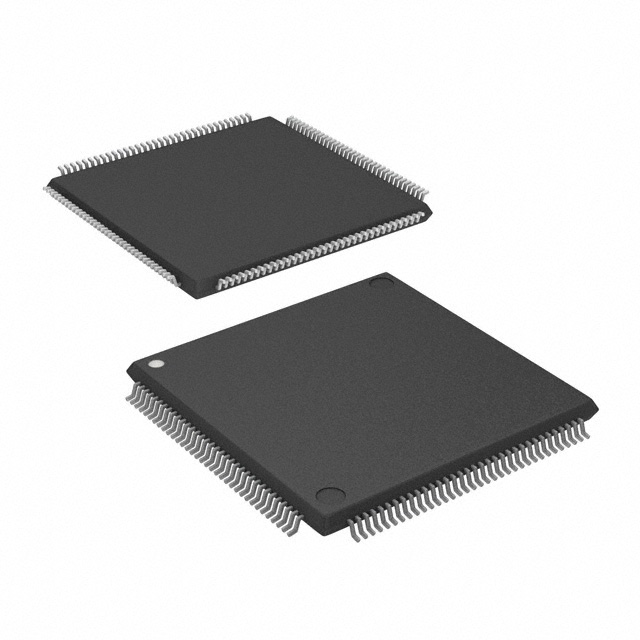
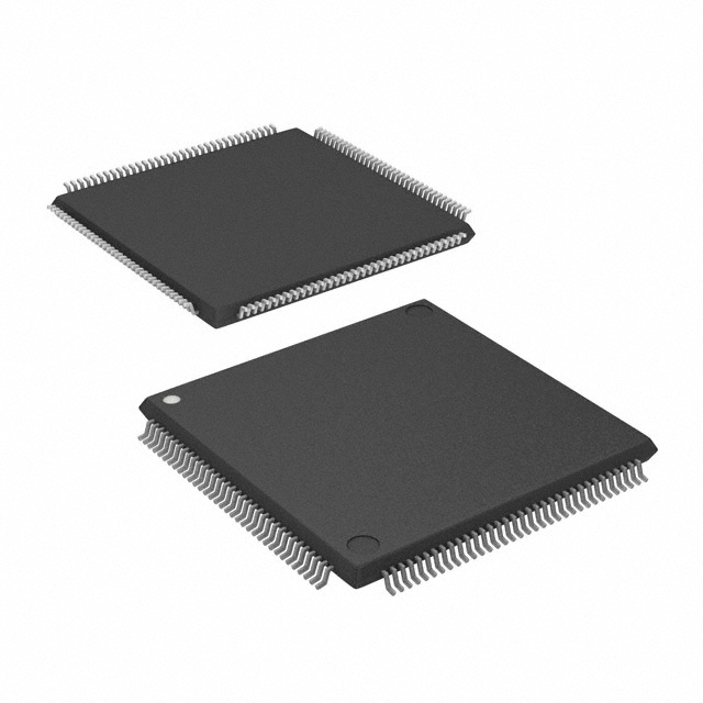
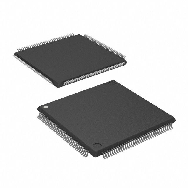
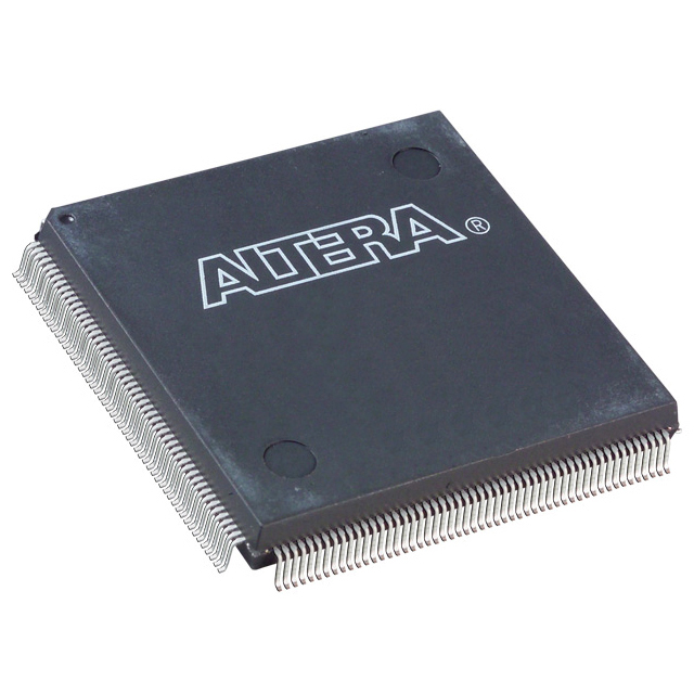
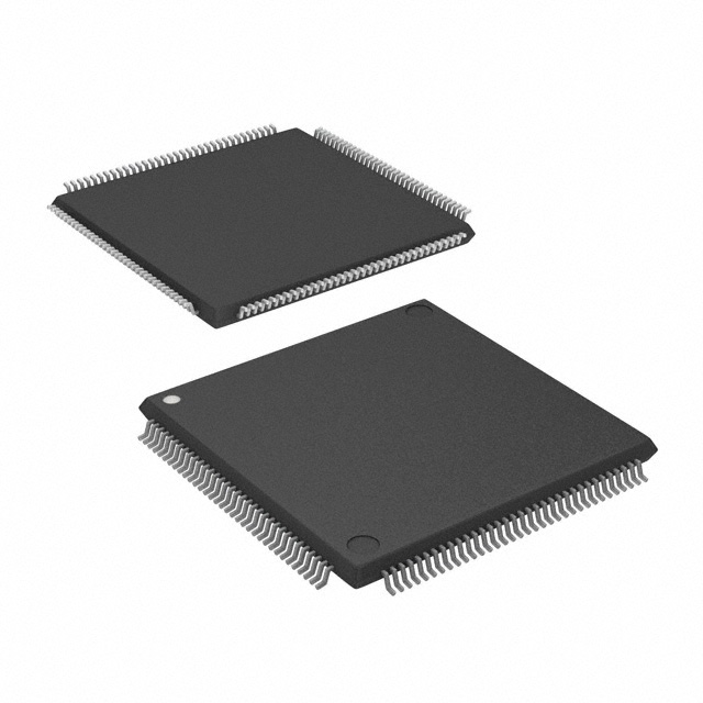
EPF6024ATC144-2N
| Part Description |
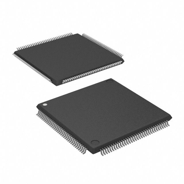
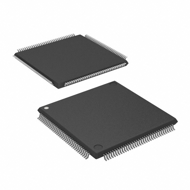
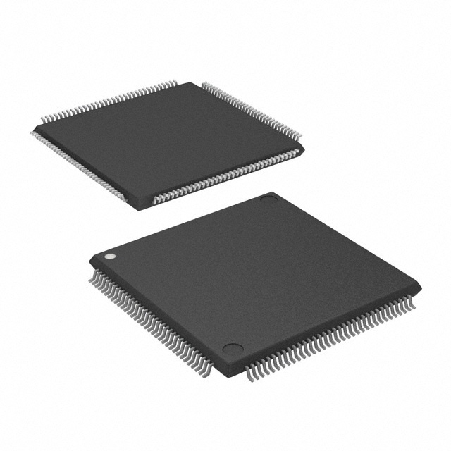
FLEX 6000 Field Programmable Gate Array (FPGA) IC 117 1960 144-LQFP |
|---|---|
| Quantity | 907 Available (as of October 8, 2026) |
| Product Category | Field Programmable Gate Array (FPGA) |
|---|---|
| Manufacturer | Intel |
| Manufacturing Status | Obsolete |
| Manufacturer Standard Lead Time | Contact Us |
| Datasheet |
Specifications & Environmental
| Device Package | 144-TQFP (20x20) | Grade | Commercial | Operating Temperature | 0°C – 85°C | ||
|---|---|---|---|---|---|---|---|
| Package / Case | 144-LQFP | Number of I/O | 117 | Voltage | 3 V - 3.6 V | ||
| Mounting Method | Surface Mount | RoHS Compliance | Unknown | REACH Compliance | REACH Unaffected | ||
| Moisture Sensitivity Level | 3 (168 Hours) | Number of LABs/CLBs | 196 | Number of Logic Elements/Cells | 1960 | ||
| Number of Gates | 24000 | ECCN | 3A001A2A | HTS Code | 8542.39.0001 | ||
| Qualification | N/A |
Overview of EPF6024ATC144-2N – FLEX 6000 Field Programmable Gate Array (FPGA) IC 117 1960 144-LQFP
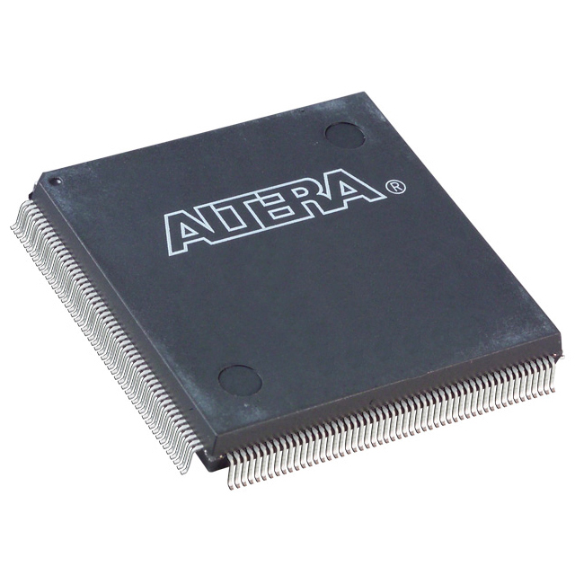
The EPF6024ATC144-2N is a FLEX 6000 family field programmable gate array (FPGA) from Intel, built on a register-rich, look-up table (LUT)-based OptiFLEX architecture. It targets low-cost, reprogrammable implementations where fast design changes, in-circuit reconfiguration and pin-compatible device scaling are important.
With 1,960 logic elements (approximately 24,000 typical gates), 117 I/O pins and a 144-pin LQFP package, this commercial-grade device is suited to prototyping, design testing and low- to mid-volume programmable logic applications that require flexible I/O and predictable routing.
Key Features
- Core architecture Register-rich, LUT-based OptiFLEX architecture that optimizes device-area efficiency and supports reprogrammable logic implementation.
- Logic capacity 1,960 logic elements (approximately 24,000 typical gates) for implementing medium-density logic functions.
- I/O and interfacing 117 I/O pins with MultiVolt I/O capability and individual tri-state output enable control; programmable output slew-rate control and a fast path from register to I/O pin for reduced clock-to-output time.
- System-level features In-circuit reconfigurability via external configuration device or intelligent controller and built-in JTAG boundary-scan (IEEE Std. 1149.1) for board-level testability.
- Dedicated arithmetic and logic chains Dedicated carry and cascade chains for efficient implementation of adders, counters and high-fan-in logic (used automatically by design tools).
- Clocking Built-in low-skew clock distribution tree and four low-skew global paths suitable for clock, clear, preset or other global control signals.
- Power and supply Supply voltage range 3 V to 3.6 V; low-power standby behavior noted in the device family documentation.
- Package and mounting 144-pin LQFP package (supplier device package 144-TQFP, 20 × 20); surface-mount mounting type for PCB assembly.
- Environmental RoHS compliant.
- Operating conditions Commercial grade with operating temperature range 0 °C to 85 °C.
Typical Applications
- Prototyping and design validation Reprogrammable fabric and in-circuit reconfiguration support rapid iteration during prototype and test phases.
- Low- to mid-volume programmable logic Medium logic capacity and flexible I/O make the device suitable for customized logic in production runs where gate arrays would otherwise be used.
- Interface bridging and mixed-voltage systems MultiVolt I/O and programmable output control facilitate bridging between subsystems operating at different supply voltages.
- Board-level test and debug Built-in JTAG boundary-scan support enables board testing and fault isolation without consuming device logic.
Unique Advantages
- Reconfigurable alternative to gate arrays: Provides a low-cost, programmable option for designs that would otherwise require custom gate-array devices, enabling fast design changes.
- Practical logic density: 1,960 logic elements (about 24,000 gates) supports medium-complexity logic blocks while keeping package and BOM overhead modest.
- Flexible I/O control: Individual tri-state enables, programmable slew-rate and MultiVolt operation simplify signal integrity and mixed-voltage interfacing.
- Built-in testability: IEEE 1149.1 JTAG boundary-scan is available without consuming user logic, aiding manufacturing test and in-field diagnostics.
- Pin- and footprint-friendly packaging: 144-pin LQFP/TQFP packaging provides a familiar surface-mount footprint for compact PCB layouts and mainstream assembly processes.
- Commercial-grade operating range: Designed for 0 °C to 85 °C operation and 3.0 V–3.6 V supply environments common in commercial embedded systems.
Why Choose EPF6024ATC144-2N?
The EPF6024ATC144-2N is positioned for designers who need a commercially graded, reprogrammable FPGA with medium logic capacity, flexible I/O and board-level test features. Its OptiFLEX architecture and dedicated arithmetic chains help implement efficient logic while preserving routing predictability.
This part is well suited to teams focused on prototyping, iterative development and low- to mid-volume production where in-circuit reconfiguration, JTAG testability and MultiVolt I/O simplify development and system integration. RoHS compliance and a standard 144-LQFP surface-mount package support mainstream manufacturing flows.
Request a quote or submit an inquiry for pricing and availability for EPF6024ATC144-2N to begin integrating this FLEX 6000 FPGA into your design.





















Date Founded: 1968
Headquarters: Santa Clara, California, USA
Employees: 130,000+
Revenue: $54.23 Billion
Certifications and Memberships: ISO9001:2015, ISO14001:2015, ISO17025:2017, ISO27001:2022, ISO45001:2018, ISO50001:2018


