
XC2V1000-4FFG896C
| Part Description |
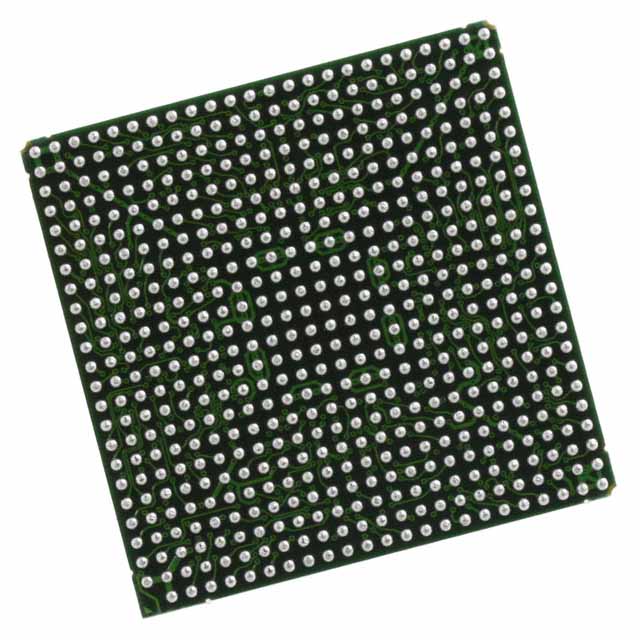
Virtex®-II Field Programmable Gate Array (FPGA) IC 432 737280 896-BBGA, FCBGA |
|---|---|
| Quantity | 1,542 Available (as of October 9, 2026) |

| Product Category | Field Programmable Gate Array (FPGA) |
|---|---|
| Manufacturer | AMD |
| Manufacturing Status | Obsolete |
| Manufacturer Standard Lead Time | Contact Us |
| Datasheet |
Specifications & Environmental
| Device Package | 896-FCBGA (31x31) | Grade | Commercial | Operating Temperature | 0°C – 85°C | ||
|---|---|---|---|---|---|---|---|
| Package / Case | 896-BBGA, FCBGA | Number of I/O | 432 | Voltage | 1.425 V - 1.575 V | ||
| Mounting Method | Surface Mount | RoHS Compliance | Unknown | REACH Compliance | REACH Unaffected | ||
| Moisture Sensitivity Level | 4 (72 Hours) | Number of LABs/CLBs | 1280 | Number of Logic Elements/Cells | 11520 | ||
| Number of Gates | 1000000 | ECCN | 3A991D | HTS Code | 8542.39.0001 | ||
| Qualification | N/A | Total RAM Bits | 737280 |
Overview of XC2V1000-4FFG896C – Virtex®-II Field Programmable Gate Array (896-FCBGA)
The XC2V1000-4FFG896C is a Virtex®-II Field Programmable Gate Array (FPGA) in a 896‑ball flip‑chip FCBGA package (31 × 31 mm). It combines programmable logic, embedded memory, and high-density I/O to support complex digital designs in commercial applications.
Designed for applications that require significant on-chip resources, the device provides 11,520 logic elements, approximately 0.737 Mbits of embedded RAM, and 432 user I/Os, while operating from a 1.425 V to 1.575 V core supply and within a 0 °C to 85 °C commercial temperature range.
Key Features
- Core Logic Provides 11,520 logic elements suitable for medium-complexity FPGA designs and system integration.
- Embedded Memory Approximately 737,280 total RAM bits of on-chip memory for data buffering, FIFOs and small shared memory structures.
- High-Density I/O 432 user I/Os accommodate extensive external interfacing and parallel connectivity.
- Arithmetic and DSP Resources Series-level architecture includes dedicated multiplier resources (18‑bit × 18‑bit multipliers) for arithmetic acceleration as described in the Virtex‑II platform documentation.
- Clock Management Support for advanced clocking functions at the platform level, including Digital Clock Manager (DCM) features documented for the Virtex‑II family.
- Package and Mounting 896‑ball flip‑chip FCBGA (31 × 31 mm), surface mount package optimized for high-density PCB designs.
- Power and Supply Core voltage specified from 1.425 V to 1.575 V to meet the device’s operating requirements.
- Operating Range Commercial grade device rated for 0 °C to 85 °C operation.
- Regulatory RoHS compliant.
Typical Applications
- High‑performance interfaces Use the XC2V1000-4FFG896C to implement DRAM/SRAM interface logic and other memory controllers that benefit from embedded RAM and dedicated multiplier resources.
- Signal processing and arithmetic acceleration Leverage on‑chip multiplier blocks and logic fabric for fixed‑function DSP tasks and custom arithmetic pipelines.
- Custom I/O and bus bridging 432 I/Os enable implementation of wide parallel interfaces, protocol bridging, or custom peripheral glue logic in commercial products.
- Embedded system control Deploy as central logic in embedded systems that require programmable control, timing management, and moderate on‑chip memory.
Unique Advantages
- Balanced resource mix: Combination of 11,520 logic elements and approximately 0.737 Mbits of embedded RAM supports designs requiring both logic density and local memory.
- High I/O count: 432 user I/Os reduce external glue logic and simplify board-level integration for multi‑bus or parallel interfaces.
- Commercial temperature rating: Rated for 0 °C to 85 °C operation to suit mainstream commercial applications.
- Compact FCBGA package: 896‑ball FCBGA (31 × 31 mm) delivers high pin density in a surface‑mount form factor for space‑constrained PCBs.
- Vendor platform capabilities: Part of the Virtex‑II platform family, which documents clock management, multiplier, and SelectRAM resources to accelerate common FPGA tasks.
- RoHS compliant: Meets lead‑free and restricted‑substance requirements for compliant product designs.
Why Choose XC2V1000-4FFG896C?
The XC2V1000-4FFG896C positions itself as a commercially rated Virtex‑II FPGA option combining a substantial logic element count, meaningful on‑chip RAM capacity, and a high I/O count in a compact flip‑chip FCBGA package. It is suited to developers building mid‑range programmable systems that require embedded memory, arithmetic acceleration, and flexible interfacing.
Choosing this device provides a balance of performance and integration for commercial embedded designs, offering a well‑documented platform of features to support development and scaling across related Virtex‑II devices.
Request a quote or submit a purchase inquiry for the XC2V1000-4FFG896C to discuss availability and pricing for your project requirements.























Date Founded: 1969
Headquarters: Santa Clara, California, USA
Employees: 25,000+
Revenue: $22.68 Billion
Certifications and Memberships: ISO9001:2015, RoHS, REACH











