
XC2V250-5FGG256C
| Part Description |
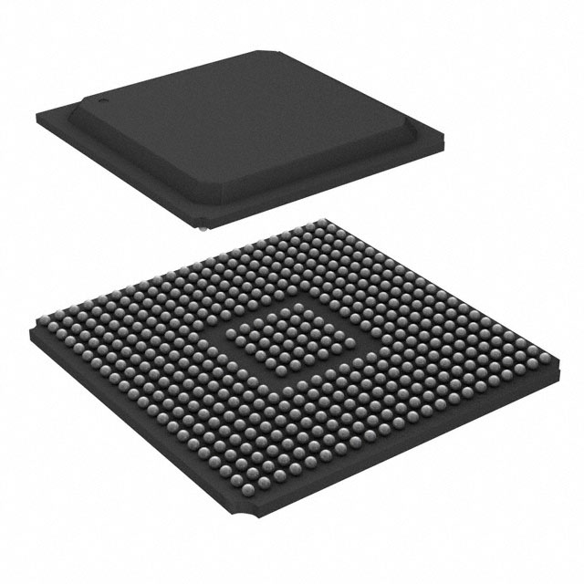
Virtex®-II Field Programmable Gate Array (FPGA) IC 172 442368 256-BGA |
|---|---|
| Quantity | 755 Available (as of June 15, 2026) |

| Product Category | Field Programmable Gate Array (FPGA) |
|---|---|
| Manufacturer | AMD |
| Manufacturing Status | Obsolete |
| Manufacturer Standard Lead Time | Contact Us |
| Datasheet |
Specifications & Environmental
| Device Package | 256-FBGA (17x17) | Grade | Commercial | Operating Temperature | 0°C – 85°C | ||
|---|---|---|---|---|---|---|---|
| Package / Case | 256-BGA | Number of I/O | 172 | Voltage | 1.425 V - 1.575 V | ||
| Mounting Method | Surface Mount | RoHS Compliance | Unknown | REACH Compliance | REACH Unaffected | ||
| Moisture Sensitivity Level | 3 (168 Hours) | Number of LABs/CLBs | 384 | Number of Logic Elements/Cells | 3456 | ||
| Number of Gates | 250000 | ECCN | 3A001A7B | HTS Code | 8542.39.0001 | ||
| Qualification | N/A | Total RAM Bits | 442368 |
Overview of XC2V250-5FGG256C – Virtex®-II FPGA, 256-BGA
The XC2V250-5FGG256C is a Virtex®-II field programmable gate array (FPGA) in a 256-ball BGA package, designed for commercial-grade applications. This device integrates programmable logic, embedded memory, dedicated multiplier resources and flexible I/O to support designs that require on-chip logic, memory and high-performance interfacing.
With 3,456 logic elements, approximately 0.42 Mbits of embedded RAM, 172 user I/Os and a 1.425 V–1.575 V core supply range, the XC2V250-5FGG256C targets system designs needing moderate gate counts, integrated arithmetic blocks and a versatile I/O footprint within a surface-mount FBGA package.
Key Features
- Logic Resources — 3,456 logic elements and 384 configurable logic blocks (CLBs) to implement custom logic and state machines.
- Gate Count — Approximately 250,000 system gates suited for mid-range FPGA designs.
- Embedded Memory — 442,368 total RAM bits (approximately 0.42 Mbits) for on-chip buffering, FIFOs and small data stores; supported by the Virtex-II SelectRAM memory hierarchy described in the datasheet.
- Dedicated Arithmetic — Series-level architecture provides 18-bit × 18-bit multiplier blocks for implementing fixed-point and DSP arithmetic (per datasheet feature set).
- I/O Capacity — 172 user I/Os in the 256-FBGA (17 × 17) footprint, enabling broad external interfacing and board-level signal routing.
- Package & Mounting — 256-BGA surface-mount package (supplier device package: 256-FBGA 17×17) for compact board integration.
- Power — Core voltage supply range of 1.425 V to 1.575 V to match system power rails and design constraints.
- Operating Range & Grade — Commercial grade with an operating temperature range of 0 °C to 85 °C.
- Environmental Compliance — RoHS compliant.
Typical Applications
- Memory Interface Controllers — Implement SDR/DDR or SRAM interface logic using the device’s embedded RAM and I/O capacity for mid-range bus bridging and memory arbitration.
- Digital Signal Processing — Use the embedded multiplier blocks and on-chip RAM for fixed-point DSP pipelines, filtering and arithmetic acceleration.
- Custom Peripheral and Bridge Logic — Integrate protocol translators, glue logic and custom peripheral controllers leveraging abundant I/Os and programmable logic.
- Prototyping and System Integration — Rapidly validate hardware architectures and integrate multiple subsystems on a single FPGA platform with moderate gate density and memory.
Unique Advantages
- Balanced Logic and Memory: 3,456 logic elements paired with approximately 0.42 Mbits of embedded memory provide a compact, integrated solution for mid-density designs.
- Dedicated Arithmetic Resources: Built-in 18-bit × 18-bit multipliers accelerate DSP and computation tasks without consuming general-purpose logic.
- Flexible I/O Count: 172 user I/Os in a 256-FBGA footprint allow broad external connectivity while keeping PCB real estate efficient.
- Commercial Temperature Rating: Specified 0 °C to 85 °C operation and commercial grade classification fit mainstream electronics and embedded applications.
- Compact Package: 256-BGA (17×17) surface-mount package simplifies board layout for space-constrained designs.
- Standards and Compliance: RoHS compliance supports current environmental requirements for commercial products.
Why Choose XC2V250-5FGG256C?
The XC2V250-5FGG256C offers a practical balance of programmable logic, on-chip RAM and arithmetic resources in a compact 256-FBGA package for commercial embedded designs. Its combination of 3,456 logic elements, dedicated multipliers and 172 I/Os makes it suitable for applications that require integrated processing, memory buffering and versatile external interfaces without moving to higher-density devices.
This device is appropriate for engineering teams seeking a commercially graded Virtex®-II platform FPGA with verifiable on-chip memory, defined power requirements and a clear operating temperature range—providing predictable integration into mid-range digital systems.
Request a quote or submit your RFQ to receive pricing and availability for the XC2V250-5FGG256C and support material to help evaluate the device for your design needs.


Date Founded: 1969
Headquarters: Santa Clara, California, USA
Employees: 25,000+
Revenue: $22.68 Billion
Certifications and Memberships: ISO9001:2015, RoHS, REACH


