
XC2V250-5FGG456I
| Part Description |
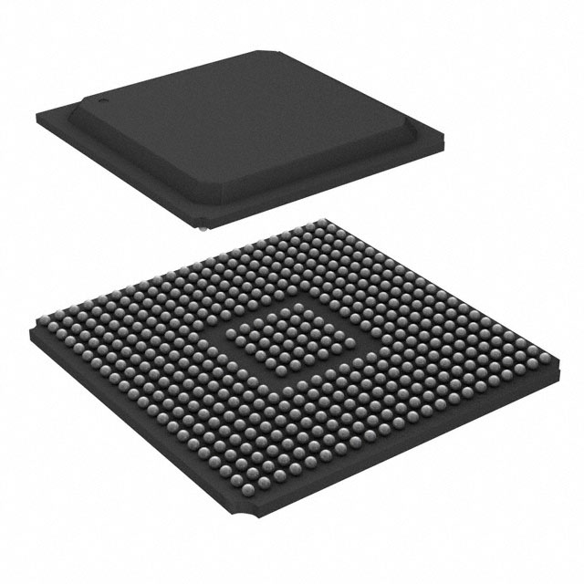
Virtex®-II Field Programmable Gate Array (FPGA) IC 200 442368 456-BBGA |
|---|---|
| Quantity | 51 Available (as of June 10, 2026) |

| Product Category | Field Programmable Gate Array (FPGA) |
|---|---|
| Manufacturer | AMD |
| Manufacturing Status | Obsolete |
| Manufacturer Standard Lead Time | Contact Us |
| Datasheet |
Specifications & Environmental
| Device Package | 456-FBGA (23x23) | Grade | Industrial | Operating Temperature | -40°C – 100°C | ||
|---|---|---|---|---|---|---|---|
| Package / Case | 456-BBGA | Number of I/O | 200 | Voltage | 1.425 V - 1.575 V | ||
| Mounting Method | Surface Mount | RoHS Compliance | Unknown | REACH Compliance | REACH Unaffected | ||
| Moisture Sensitivity Level | 3 (168 Hours) | Number of LABs/CLBs | 384 | Number of Logic Elements/Cells | 3456 | ||
| Number of Gates | 250000 | ECCN | 3A991D | HTS Code | 8542.39.0001 | ||
| Qualification | N/A | Total RAM Bits | 442368 |
Overview of XC2V250-5FGG456I – Virtex®-II Field Programmable Gate Array (FPGA) IC 200 442368 456-BBGA
The XC2V250-5FGG456I is a Virtex®-II platform FPGA offering a mid-range fabric density with industry-oriented specifications. Built on the Virtex-II architecture, this device provides flexible logic resources, embedded memory, and a versatile I/O complement for system designs that require on-chip RAM, dedicated arithmetic blocks, and configurable clock management.
Targeted for industrial applications, the device delivers a combination of logic capacity, embedded memory and I/O count in a 456-ball BGA package, with supply and thermal ranges suited for ruggedized deployments.
Key Features
- Logic Capacity — 3,456 logic elements delivered via 384 CLBs (configurable logic blocks) for implementing combinational and sequential logic.
- Embedded Memory — Approximately 0.44 Mbits of on-chip RAM (442,368 bits) for data buffering, state storage and small memory arrays.
- Dedicated Arithmetic — Series-level support for 18-bit × 18-bit multiplier blocks provides hardware acceleration for DSP and arithmetic-intensive functions.
- I/O and Package — 200 user I/Os in a 456-BBGA package (supplier device package: 456-FBGA, 23×23) to accommodate board-level routing and dense interconnect requirements.
- Power Supply — Core voltage range specified at 1.425 V to 1.575 V for predictable power design and decoupling.
- Clock Management — Includes Digital Clock Manager (DCM) functionality (series capability) for clock de-skew, phase shifting and frequency synthesis.
- Industrial Temperature Grade — Rated for operation from −40 °C to 100 °C, suitable for industrial temperature environments.
- RoHS Compliance — Device is RoHS compliant.
Typical Applications
- Communications and Networking — Use the device’s dedicated multipliers and embedded memory for packet processing, framing logic and memory buffering in network equipment.
- Embedded Control Systems — Ideal for industrial controllers requiring deterministic logic, on-chip RAM for state machines and broad I/O for sensor/actuator interfaces.
- Test & Measurement — Leverage high logic density and configurable I/O to implement custom data capture, pre-processing and timing control.
Unique Advantages
- Balanced Logic and Memory — The mix of 3,456 logic elements and approximately 0.44 Mbits of embedded RAM enables compact implementations without external memory for many functions.
- Hardware DSP Support — Integrated 18-bit × 18-bit multiplier blocks accelerate arithmetic and signal-processing tasks, reducing reliance on external DSP components.
- Robust Industrial Operation — Rated for −40 °C to 100 °C operation, supporting deployment in harsh or temperature-variable environments.
- High I/O Count in Compact BGA — 200 I/O pins in a 456-ball BGA (23×23) package simplify board-level connectivity while keeping PCB area efficient.
- Predictable Power Requirements — Defined core voltage window (1.425 V to 1.575 V) helps streamline power-supply design and validation.
Why Choose XC2V250-5FGG456I?
The XC2V250-5FGG456I positions itself as a practical FPGA choice where a balance of logic resources, embedded memory and I/O density is required within an industrial temperature envelope. Its Virtex‑II series architecture provides proven infrastructure for clock management and hardware multiplication, enabling designers to consolidate functions on a single device and reduce external component count.
This device is well suited to engineers designing industrial control, communications, or measurement systems who need a reliable, mid-range FPGA offering specific, verifiable specifications for logic elements, on-chip RAM and I/O in a compact BGA package.
Request a quote or submit an inquiry to receive pricing and availability information for the XC2V250-5FGG456I. Our team can provide lead-time details and support for your design evaluation needs.


Date Founded: 1969
Headquarters: Santa Clara, California, USA
Employees: 25,000+
Revenue: $22.68 Billion
Certifications and Memberships: ISO9001:2015, RoHS, REACH


