
XC2V250-6FGG256C
| Part Description |
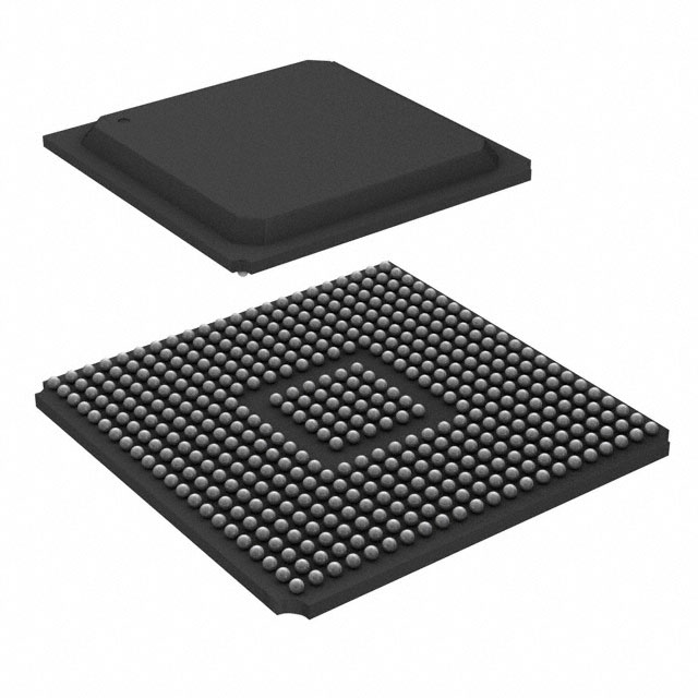
Virtex®-II Field Programmable Gate Array (FPGA) IC 172 442368 256-BGA |
|---|---|
| Quantity | 637 Available (as of June 18, 2026) |

| Product Category | Field Programmable Gate Array (FPGA) |
|---|---|
| Manufacturer | AMD |
| Manufacturing Status | Obsolete |
| Manufacturer Standard Lead Time | Contact Us |
| Datasheet |
Specifications & Environmental
| Device Package | 256-FBGA (17x17) | Grade | Commercial | Operating Temperature | 0°C – 85°C | ||
|---|---|---|---|---|---|---|---|
| Package / Case | 256-BGA | Number of I/O | 172 | Voltage | 1.425 V - 1.575 V | ||
| Mounting Method | Surface Mount | RoHS Compliance | Unknown | REACH Compliance | REACH Unaffected | ||
| Moisture Sensitivity Level | 3 (168 Hours) | Number of LABs/CLBs | 384 | Number of Logic Elements/Cells | 3456 | ||
| Number of Gates | 250000 | ECCN | 3A001A7B | HTS Code | 8542.39.0001 | ||
| Qualification | N/A | Total RAM Bits | 442368 |
Overview of XC2V250-6FGG256C – Virtex®-II FPGA, 256‑BGA, 172 I/Os
The XC2V250-6FGG256C is a Virtex®-II field programmable gate array (FPGA) in a 256‑ball BGA package, designed for commercial embedded applications. Based on the Virtex‑II platform, this device combines configurable logic, embedded RAM, and a high‑density I/O count to support custom digital logic, memory interface, and data‑processing functions.
With 3,456 logic elements and approximately 0.42 Mbits of on‑chip RAM, the XC2V250-6FGG256C targets designs that require moderate logic density, dedicated embedded memory, and flexible I/O connectivity within a surface‑mount 256‑FBGA (17×17) footprint.
Key Features
- Logic Capacity Provides 3,456 logic elements enabling implementation of custom digital functions and moderate-complexity designs.
- Embedded Memory Approximately 0.42 Mbits (442,368 bits) of on‑chip RAM for buffer, FIFO, and local storage needs.
- I/O Resources 172 user I/Os to support multi‑lane interfaces, peripheral control, and board-level connectivity.
- Gate Equivalent Rated at 250,000 gates for capacity planning and architecture comparisons.
- Package & Mounting 256‑ball BGA (Supplier device package: 256‑FBGA, 17×17) in a surface‑mount form factor for compact system integration.
- Power Supply Core voltage specified at 1.425 V to 1.575 V.
- Operating Range Commercial temperature grade: 0 °C to 85 °C.
- Regulatory RoHS compliant.
- Platform Capabilities (Virtex‑II) The Virtex‑II family provides features such as SelectRAM block memories, dedicated multiplier blocks, and clock management resources for designs that require memory hierarchy, arithmetic acceleration, and precise clocking (see full Virtex‑II documentation for series‑level details).
Typical Applications
- Memory Interface and Bridge Logic: Implement SDR/DDR or SRAM interface controllers and glue logic using the device's embedded RAM and I/O density.
- Signal and Data Processing: Use the on‑chip RAM and logic resources for buffering, packet handling, or moderate arithmetic acceleration tasks.
- Custom Digital Systems: Ideal for prototyping and deploying custom control, glue, or protocol conversion logic in commercial embedded products.
- Board‑Level I/O Concentration: High I/O count supports multi‑channel sensor aggregation, peripheral interfacing, or multi‑lane connectivity on compact PCBs.
Unique Advantages
- Balanced Logic and Memory: Combines 3,456 logic elements with approximately 0.42 Mbits of embedded RAM to support both control logic and local data storage in a single device.
- High I/O Density: 172 I/Os reduce the need for external glue logic and simplify board routing for multi‑interface designs.
- Compact Surface‑Mount Package: 256‑FBGA (17×17) enables high‑density integration in space‑constrained commercial products.
- Commercial Temperature Grade: Rated for 0 °C to 85 °C operation to match typical commercial embedded system environments.
- Standards‑Aware Platform: As part of the Virtex‑II family, the device is aligned with platform features such as block SelectRAM and dedicated multipliers for designs that need memory hierarchy and arithmetic support (refer to Virtex‑II series documentation for details).
- RoHS Compliance: Meets RoHS requirements for environmentally conscious manufacturing and assembly.
Why Choose XC2V250-6FGG256C?
The XC2V250-6FGG256C delivers a practical balance of logic capacity, embedded RAM, and a high I/O count in a compact 256‑ball FBGA package for commercial embedded designs. It is well suited to teams that need configurable logic with built‑in memory and board‑level I/O consolidation without moving to larger, higher‑cost FPGA tiers.
Designed around the Virtex‑II platform, this device offers architecture and series‑level capabilities that support memory interfaces, arithmetic functions, and precise clock management—providing a predictable integration path for moderate‑complexity applications that value integration and reuse of platform features.
Request a quote or submit a pricing inquiry to receive availability and lead time information for XC2V250-6FGG256C. Our sales team will provide a formal quote and support your procurement and design planning needs.


Date Founded: 1969
Headquarters: Santa Clara, California, USA
Employees: 25,000+
Revenue: $22.68 Billion
Certifications and Memberships: ISO9001:2015, RoHS, REACH


