
XC2V250-6FG256C
| Part Description |
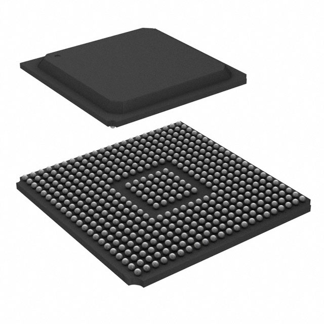
Virtex®-II Field Programmable Gate Array (FPGA) IC 172 442368 256-BGA |
|---|---|
| Quantity | 1,091 Available (as of June 14, 2026) |

| Product Category | Field Programmable Gate Array (FPGA) |
|---|---|
| Manufacturer | AMD |
| Manufacturing Status | Obsolete |
| Manufacturer Standard Lead Time | Contact Us |
| Datasheet |
Specifications & Environmental
| Device Package | 256-FBGA (17x17) | Grade | Commercial | Operating Temperature | 0°C – 85°C | ||
|---|---|---|---|---|---|---|---|
| Package / Case | 256-BGA | Number of I/O | 172 | Voltage | 1.425 V - 1.575 V | ||
| Mounting Method | Surface Mount | RoHS Compliance | Unknown | REACH Compliance | REACH Unaffected | ||
| Moisture Sensitivity Level | 3 (168 Hours) | Number of LABs/CLBs | 384 | Number of Logic Elements/Cells | 3456 | ||
| Number of Gates | 250000 | ECCN | 3A001A7B | HTS Code | 8542.39.0001 | ||
| Qualification | N/A | Total RAM Bits | 442368 |
Overview of XC2V250-6FG256C – Virtex®-II Field Programmable Gate Array (FPGA) IC 172 442368 256-BGA
The XC2V250-6FG256C is a Virtex®-II platform field programmable gate array supplied by AMD. It delivers a balanced combination of configurable logic, embedded memory, and flexible I/O in a 256-ball BGA package suitable for commercial-grade designs.
Designed for applications that require on-chip RAM, dedicated arithmetic resources and a high density of I/O, this device supports implementation of custom logic, memory interfaces and signal-processing functions while operating within a 1.425 V to 1.575 V supply range and a 0 °C to 85 °C commercial temperature window.
Key Features
- Virtex®-II platform architecture Series-level IP-Immersion architecture providing the established feature set of Virtex-II devices, including configurable logic, clock management and SelectRAM memory hierarchy.
- Logic capacity Approximately 3,456 logic elements and 250,000 system gates allow implementation of moderate-complexity custom logic functions.
- Embedded memory Approximately 0.44 Mbits (442,368 bits) of on-chip RAM to support data buffering, state storage and memory-intensive logic without immediate external RAM.
- I/O resources 172 user I/O pins in a fine-pitch 256-ball BGA footprint provide flexible external interfacing for peripherals, memories and transceivers; the Virtex-II series supports a broad set of I/O standards.
- Arithmetic and DSP support Series features include dedicated 18-bit × 18-bit multiplier blocks and fast carry chains for hardware-accelerated multiply and arithmetic operations.
- Clock management Virtex-II devices include Digital Clock Manager (DCM) functionality and global clock routing to help meet timing and synchronization needs in complex designs.
- Package and mounting 256‑FBGA (17 × 17) surface-mount package (256-BGA) for compact board integration and reliable solder mounting.
- Electrical and environmental Specified supply voltage range: 1.425 V to 1.575 V. Commercial-grade operating temperature range: 0 °C to 85 °C. RoHS compliant.
Typical Applications
- Memory interface controllers On-chip RAM and flexible I/O make this device suitable for building SDR/DDR memory interfaces and buffering logic in embedded systems.
- Signal processing and DSP blocks Dedicated multiplier resources and look-ahead carry chains support hardware acceleration of arithmetic and filtering algorithms.
- Communications and protocol bridging High I/O count and Virtex-II series SelectIO capabilities enable protocol conversion, bus bridging and front-end interface logic.
- Custom logic and prototyping The combination of logic elements and embedded RAM is well suited for implementing custom control logic, state machines and medium-complexity prototypes.
Unique Advantages
- Balanced integration: Combines thousands of logic elements with approximately 0.44 Mbits of embedded RAM to reduce dependency on external memory for many mid-range designs.
- Flexible external interfacing: 172 user I/Os in a 256‑FBGA footprint provide broad connectivity options for sensors, memories and peripheral devices.
- Hardware arithmetic acceleration: Series-level dedicated multiplier blocks enable efficient implementation of multiply-intensive functions without consuming general-purpose logic.
- Commercial-grade robustness: Specified operating range of 0 °C to 85 °C and RoHS compliance align with typical commercial product requirements.
- Compact board integration: Surface-mount 256‑FBGA (17 × 17) package supports dense PCB layouts while maintaining reliable solder mounting.
Why Choose XC2V250-6FG256C?
The XC2V250-6FG256C offers a practical balance of logic capacity, embedded memory and I/O resources in a compact BGA package, making it a capable choice for commercial embedded designs that need moderate logic density combined with on-chip RAM and dedicated arithmetic support. Its Virtex-II platform heritage provides a familiar architecture for teams implementing clock management, memory interfacing and signal-processing functions.
Choose this device when you need a commercially graded FPGA solution with defined supply and temperature ranges, RoHS compliance, and the series-level feature set of the Virtex-II family to accelerate development of custom digital logic and interfacing solutions.
Request a quote or submit a quote to check availability and pricing for XC2V250-6FG256C.


Date Founded: 1969
Headquarters: Santa Clara, California, USA
Employees: 25,000+
Revenue: $22.68 Billion
Certifications and Memberships: ISO9001:2015, RoHS, REACH


