
XC2VP20-6FFG896C
| Part Description |
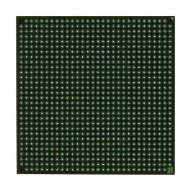
Virtex®-II Pro Field Programmable Gate Array (FPGA) IC 556 1622016 20880 896-BBGA, FCBGA |
|---|---|
| Quantity | 538 Available (as of October 8, 2026) |

| Product Category | Field Programmable Gate Array (FPGA) |
|---|---|
| Manufacturer | AMD |
| Manufacturing Status | Obsolete |
| Manufacturer Standard Lead Time | Contact Us |
| Datasheet |
Specifications & Environmental
| Device Package | 896-FCBGA (31x31) | Grade | Commercial | Operating Temperature | 0°C – 85°C | ||
|---|---|---|---|---|---|---|---|
| Package / Case | 896-BBGA, FCBGA | Number of I/O | 556 | Voltage | 1.425 V - 1.575 V | ||
| Mounting Method | Surface Mount | RoHS Compliance | ROHS3 Compliant | REACH Compliance | REACH Unaffected | ||
| Moisture Sensitivity Level | 4 (72 Hours) | Number of LABs/CLBs | 2320 | Number of Logic Elements/Cells | 20880 | ||
| Number of Gates | N/A | ECCN | 3A001A7A | HTS Code | 8542.39.0001 | ||
| Qualification | N/A | Total RAM Bits | 1622016 |
Overview of XC2VP20-6FFG896C – Virtex®-II Pro FPGA, 896-FCBGA
The XC2VP20-6FFG896C is a Virtex®-II Pro field programmable gate array (FPGA) from AMD, supplied in an 896-ball flip-chip BGA (896-FCBGA, 31×31) package. It delivers a balanced combination of programmable logic, embedded memory, and high I/O density for demanding embedded and communications-oriented designs.
Built on the Virtex-II Pro platform, this device targets applications that require substantial on-chip logic and memory, extensive I/O connectivity, and platform-level support such as IP cores and reference materials found in the Virtex-II Pro family documentation.
Key Features
- Logic Capacity — 20,880 logic elements to implement complex custom logic and control functions.
- Embedded Memory — Approximately 1.62 Mbits of on-chip RAM for buffering, lookup tables, and local data storage.
- I/O Density — 556 user I/O pins to support high-pin-count interfaces and multi-channel connectivity.
- Package — 896-ball flip-chip BGA (896-FCBGA) in a 31×31 footprint, optimized for surface-mount PCB assembly.
- Power and Thermal — Core supply range from 1.425 V to 1.575 V and specified commercial operating temperature range of 0 °C to 85 °C.
- On-chip Resources (Platform) — As part of the Virtex-II Pro family, platform features include embedded processor block options, multi-gigabit transceiver support, dedicated 18×18 multipliers, digital clock management, and a SelectRAM™ memory hierarchy (refer to family documentation for details).
- Regulatory — RoHS-compliant for environmental and regulatory alignment.
Typical Applications
- Telecom & Datacom Interfaces — Use the high I/O count and family-level transceiver resources for protocol bridging, line cards, and data path processing.
- Embedded Processing Systems — Combine programmable logic with on-chip processing resources and memory to implement control planes and custom accelerators.
- High-density I/O Systems — Leverage 556 I/O pins and a compact 896-FCBGA package for multi-channel interface aggregation and board-level integration.
- Prototyping & System Integration — Suitable for development of custom logic and system prototyping where substantial logic and embedded memory are required.
Unique Advantages
- High Logic Density: 20,880 logic elements enable implementation of substantial custom logic functions without external gate arrays.
- Significant On-chip Memory: Approximately 1.62 Mbits of embedded RAM reduces dependence on external memory for many buffering and LUT needs.
- Extensive I/O: 556 I/O pins support broad interface options and simplify routing for multi-channel designs.
- Compact, Assembly-friendly Package: 896-FCBGA (31×31) provides high ball count in a compact footprint for dense PCB layouts.
- Platform-level Resources: Access to Virtex-II Pro family features such as embedded processor blocks, transceiver capabilities, and dedicated multipliers helps accelerate system-level design.
- Commercial-grade Specification: Rated for 0 °C to 85 °C operation with RoHS compliance for mainstream embedded and communications products.
Why Choose XC2VP20-6FFG896C?
The XC2VP20-6FFG896C positions itself as a versatile Virtex®-II Pro platform device that balances logic capacity, embedded memory, and high I/O count in a compact 896-FCBGA package. It is well suited for engineers and teams building embedded processing, communications, and high-density I/O systems that benefit from on-chip resources and platform-level documentation and IP support.
With defined core voltage requirements and a commercial operating temperature range, this device provides predictable electrical and thermal requirements for production designs while maintaining environmental compliance through RoHS alignment.
If you would like pricing, availability, or to submit a quote request for XC2VP20-6FFG896C, please request a quote or submit an inquiry and our team will respond with the next steps.
























Date Founded: 1969
Headquarters: Santa Clara, California, USA
Employees: 25,000+
Revenue: $22.68 Billion
Certifications and Memberships: ISO9001:2015, RoHS, REACH











