
XC2VP30-5FG676C
| Part Description |
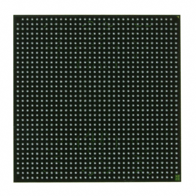
Virtex®-II Pro Field Programmable Gate Array (FPGA) IC 416 2506752 30816 676-BGA |
|---|---|
| Quantity | 561 Available (as of June 18, 2026) |

| Product Category | Field Programmable Gate Array (FPGA) |
|---|---|
| Manufacturer | AMD |
| Manufacturing Status | Obsolete |
| Manufacturer Standard Lead Time | Contact Us |
| Datasheet |
Specifications & Environmental
| Device Package | 676-FBGA (27x27) | Grade | Commercial | Operating Temperature | 0°C – 85°C | ||
|---|---|---|---|---|---|---|---|
| Package / Case | 676-BGA | Number of I/O | 416 | Voltage | 1.425 V - 1.575 V | ||
| Mounting Method | Surface Mount | RoHS Compliance | RoHS non-compliant | REACH Compliance | REACH Unaffected | ||
| Moisture Sensitivity Level | 3 (168 Hours) | Number of LABs/CLBs | 3424 | Number of Logic Elements/Cells | 30816 | ||
| Number of Gates | N/A | ECCN | 3A001A7A | HTS Code | 8542.39.0001 | ||
| Qualification | N/A | Total RAM Bits | 2506752 |
Overview of XC2VP30-5FG676C – Virtex®-II Pro Field Programmable Gate Array (676-BGA)
The XC2VP30-5FG676C is a Virtex®-II Pro FPGA IC from AMD, delivered in a 676-ball fine-pitch BGA (27 × 27 mm) package for surface-mount assembly. It provides high logic density and extensive I/O in a commercial-grade FPGA intended for embedded and high-density logic applications.
With roughly 30,816 logic elements and approximately 2.5 Mbits of embedded RAM, this device targets designs that require substantial on-chip memory, flexible logic resources, and large I/O counts while operating within a 0 °C to 85 °C commercial temperature range.
Key Features
- Logic Capacity Approximately 30.8k logic elements (30,816 logic cells) to implement complex digital functions and control logic.
- Embedded Memory Approximately 2.5 Mbits of on-chip RAM for buffering, state storage, and algorithmic working memory.
- I/O Density 416 user I/Os to support multiple interfaces, parallel buses, and wide data paths at the board level.
- Power and Supply Core supply range 1.425 V to 1.575 V for the FPGA core power domain.
- Package & Mounting 676-FBGA (27 × 27 mm) package case in a surface-mount format for compact, high-density board designs.
- Operating Conditions Commercial grade device rated for 0 °C to 85 °C operation.
- Compliance RoHS compliant for environmental and regulatory alignment.
- Virtex-II Pro Family Capabilities The Virtex-II Pro family datasheet documents platform-level features such as embedded PowerPC processor blocks and RocketIO multi-gigabit transceivers, along with dedicated 18 × 18 multiplier blocks and advanced clock management—refer to the datasheet for device-specific availability and configuration options.
Typical Applications
- High-performance communications Used where dense logic and large I/O counts are needed to implement protocol bridging, packet processing, or interface aggregation—family transceiver and platform features support telecom/datacom designs (see datasheet for device-level options).
- Embedded processing Suitable for systems that combine custom logic with embedded processors or soft cores, leveraging on-chip memory and logic capacity for control and data-path tasks.
- DSP and acceleration On-chip RAM and dedicated multiplier resources make the device appropriate for signal processing, filtering, and hardware-accelerated computation blocks.
- Custom I/O and interface bridging Large 416-pin I/O availability supports multiple parallel interfaces, sensor arrays, or wide data buses for board-level integration.
Unique Advantages
- High logic density: About 30,816 logic elements enable implementation of complex state machines, datapaths, and glue logic in a single device.
- Substantial on-chip memory: Approximately 2.5 Mbits of embedded RAM reduces external memory dependence and simplifies data buffering and packet handling.
- Extensive I/O count: 416 I/Os provide flexibility for multi-interface designs and dense board-level connectivity.
- Compact BGA packaging: 676-FBGA (27 × 27 mm) supports high-density PCB layouts while maintaining a surface-mount footprint.
- Commercial-grade reliability: Specified for 0 °C to 85 °C operation and RoHS compliance, suitable for a wide range of commercial embedded products.
- Platform heritage: Based on the Virtex-II Pro family platform; consult the datasheet for family-level capabilities such as embedded processor blocks and multi-gigabit transceiver options.
Why Choose XC2VP30-5FG676C?
The XC2VP30-5FG676C balances high logic capacity, meaningful embedded memory, and a large I/O complement in a compact 676-FBGA package, making it a strong choice for commercial embedded designs that demand on-chip resources and flexible interfacing. Its Virtex-II Pro platform lineage provides documented capabilities—such as dedicated multipliers, clock management, and optional processor/transceiver blocks—backed by an established datasheet and design guidance.
This device is well suited to teams implementing systems that require significant on-chip logic and memory while retaining flexibility for interface-rich board designs. The combination of density, package footprint, and RoHS compliance supports robust, scalable deployments in commercial products.
Request a quote or submit a quote today to evaluate the XC2VP30-5FG676C for your next high-density embedded FPGA design.


Date Founded: 1969
Headquarters: Santa Clara, California, USA
Employees: 25,000+
Revenue: $22.68 Billion
Certifications and Memberships: ISO9001:2015, RoHS, REACH


