
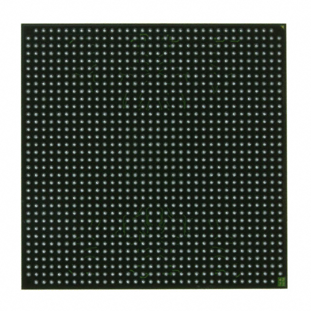
XC2VP30-5FFG1152C
| Part Description |
Virtex®-II Pro Field Programmable Gate Array (FPGA) IC 644 2506752 30816 1152-BBGA, FCBGA |
|---|---|
| Quantity | 1,541 Available (as of October 8, 2026) |

| Product Category | Field Programmable Gate Array (FPGA) |
|---|---|
| Manufacturer | AMD |
| Manufacturing Status | Obsolete |
| Manufacturer Standard Lead Time | Contact Us |
| Datasheet |
Specifications & Environmental
| Device Package | 1152-FCBGA (35x35) | Grade | Commercial | Operating Temperature | 0°C – 85°C | ||
|---|---|---|---|---|---|---|---|
| Package / Case | 1152-BBGA, FCBGA | Number of I/O | 644 | Voltage | 1.425 V - 1.575 V | ||
| Mounting Method | Surface Mount | RoHS Compliance | ROHS3 Compliant | REACH Compliance | REACH Unaffected | ||
| Moisture Sensitivity Level | 4 (72 Hours) | Number of LABs/CLBs | 3424 | Number of Logic Elements/Cells | 30816 | ||
| Number of Gates | N/A | ECCN | 3A001A7A | HTS Code | 8542.39.0001 | ||
| Qualification | N/A | Total RAM Bits | 2506752 |
Overview of XC2VP30-5FFG1152C – Virtex®-II Pro FPGA, 1152-FCBGA
The XC2VP30-5FFG1152C is a Virtex®-II Pro field programmable gate array (FPGA) in a 1152-ball FCBGA package, designed as a platform FPGA solution with integrated system-level resources. It provides a high I/O count and substantial embedded memory and logic capacity for applications that require dense, reconfigurable logic, on-chip RAM, and platform-level integration.
This commercial-grade device targets telecom/datacom and embedded processing markets where in-system configurability, abundant I/O, and processor/transceiver integration are valuable. Family-level architecture includes embedded processor blocks and RocketIO multi-gigabit transceiver capabilities for advanced system integration.
Key Features
- Logic Resources Approximately 30,816 logic elements to implement complex glue logic, control, and custom processing functions.
- Embedded Memory Approximately 2.5 Mbits of on-chip RAM (total RAM bits: 2,506,752) for buffering, packet storage, and local data handling.
- I/O Capacity Up to 644 user I/O pins, enabling extensive parallel interfaces and high-density board-level connectivity.
- Processor & Transceiver Integration (Family Features) Virtex-II Pro family devices can include up to two IBM PowerPC RISC processor blocks and up to twenty RocketIO or RocketIO X embedded multi-gigabit transceivers for embedded processing and high-speed serial connectivity (family-level capability specified in the product datasheet).
- Dedicated DSP Primitives (Family Features) Dedicated 18-bit × 18-bit multiplier blocks and 18-Kb block SelectRAM resources are part of the Virtex-II Pro family architecture for efficient arithmetic and memory-intensive functions.
- Package & Mounting 1152-ball FCBGA package (1152-FCBGA, 35×35) in a surface-mount form factor to support compact, high-density board designs.
- Supply & Temperature Operating voltage range 1.425 V to 1.575 V and commercial temperature range 0 °C to 85 °C, suitable for standard commercial embedded systems.
- Compliance RoHS compliant, supporting regulatory requirements for lead-free assemblies.
Typical Applications
- Telecom / Datacom Systems Use the device’s family-level RocketIO transceiver capabilities and high I/O count for packet processing, framer/deframer logic, and interface bridging in communications equipment.
- Embedded Processing Platforms Leverage the Virtex-II Pro family’s integrated PowerPC processor blocks and abundant logic/memory resources for control plane or application-specific acceleration tasks.
- High-Density Interface Aggregation Deploy the 644 I/O pins and extensive logic fabric to consolidate multiple parallel interfaces and protocol translators on a single FPGA.
- Custom DSP and Acceleration Apply the device’s dedicated multiplier blocks and block RAM resources to implement fixed-point DSP pipelines, filters, and hardware accelerators.
Unique Advantages
- Platform-Level Integration: Embedded processor block and RocketIO transceiver support at the family level reduce external component count and simplify system architecture.
- High I/O Density: 644 I/Os enable direct connections to multiple peripherals and parallel buses without extensive glue logic.
- Substantial On-Chip Memory: Approximately 2.5 Mbits of embedded RAM provide local buffering and state storage for latency-sensitive designs.
- Compact FCBGA Package: 1152-ball FCBGA (35×35) supports high pin count in a compact footprint for space-constrained boards.
- Commercial-Grade Reliability: Specified for 0 °C to 85 °C operation and RoHS compliance to align with commercial product requirements and environmental regulations.
Why Choose XC2VP30-5FFG1152C?
The XC2VP30-5FFG1152C combines a large logic element count, multi-megabit embedded RAM, and a very high I/O count in a compact FCBGA package, making it suitable for commercial embedded systems that require dense, reconfigurable logic and extensive board-level connectivity. Family-level features described in the product datasheet—such as integrated PowerPC processor blocks and RocketIO transceivers—support advanced system integration and reduce external component needs.
This device is a strong option for engineers designing telecom/datacom equipment, embedded processing platforms, or high-density interface aggregation solutions where platform-level FPGA capabilities and on-chip resources translate directly to reduced BOM complexity and faster time to market.
Request a quote or submit a sales inquiry to learn more about availability, pricing, and lead times for the XC2VP30-5FFG1152C. Our team can provide procurement details and help assess suitability for your design.

























Date Founded: 1969
Headquarters: Santa Clara, California, USA
Employees: 25,000+
Revenue: $22.68 Billion
Certifications and Memberships: ISO9001:2015, RoHS, REACH











