
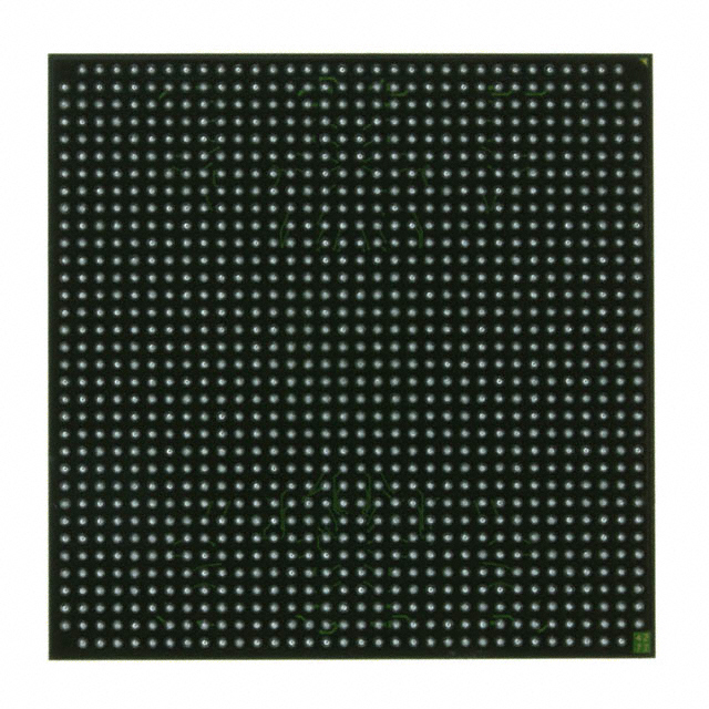
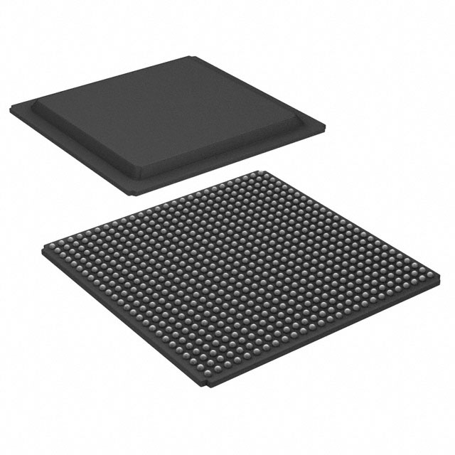
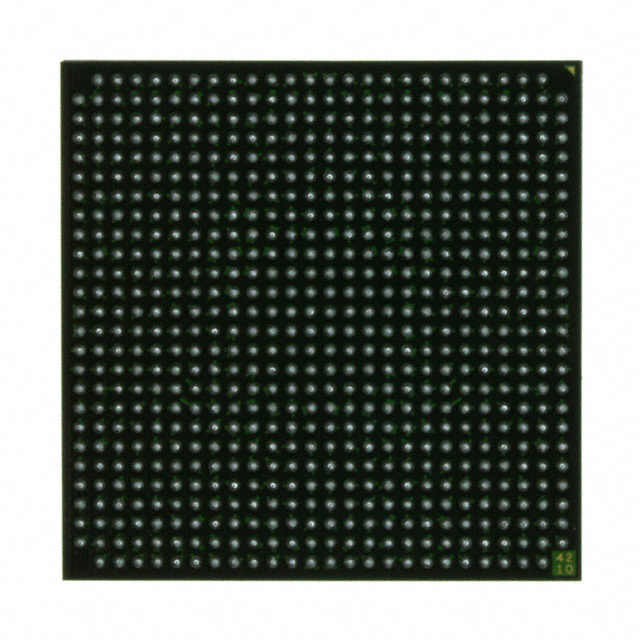
XC2VP30-7FF1152C
| Part Description |
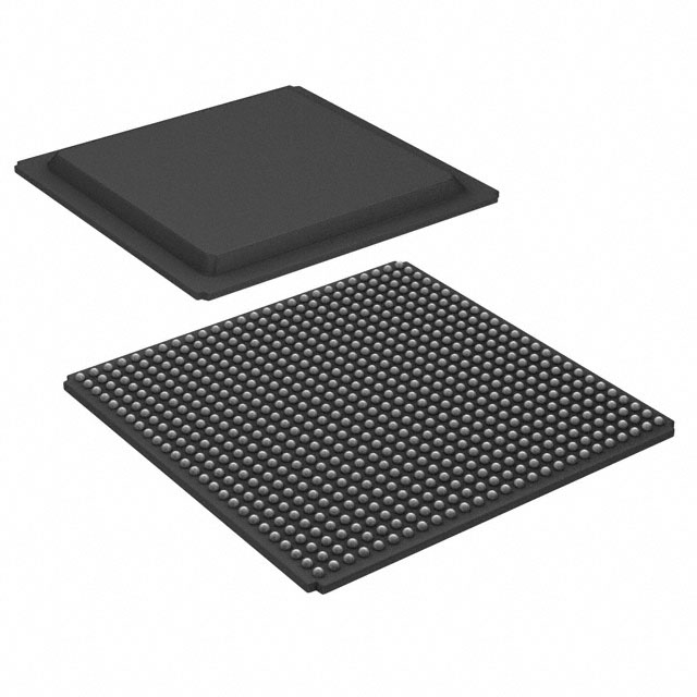
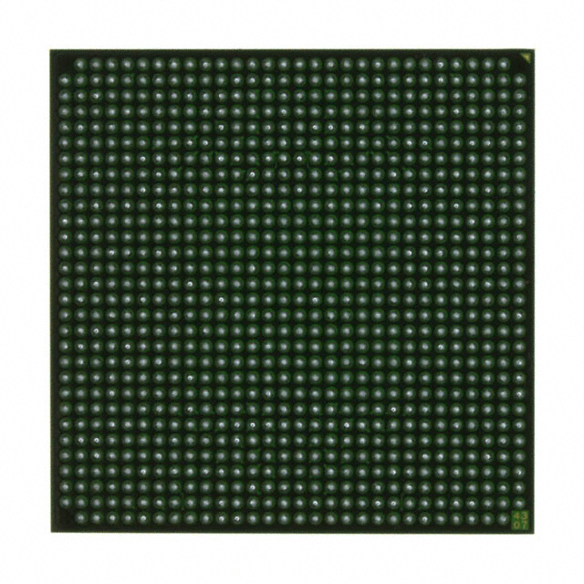
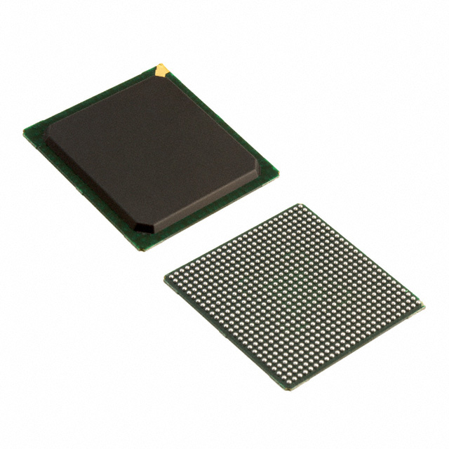
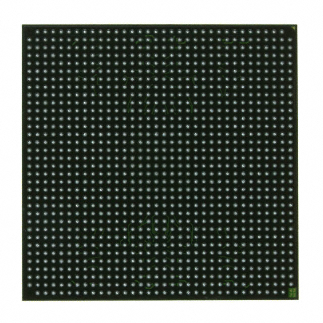
Virtex®-II Pro Field Programmable Gate Array (FPGA) IC 644 2506752 30816 1152-BBGA, FCBGA |
|---|---|
| Quantity | 898 Available (as of October 7, 2026) |
| Product Category | Field Programmable Gate Array (FPGA) |
|---|---|
| Manufacturer | AMD |
| Manufacturing Status | Obsolete |
| Manufacturer Standard Lead Time | Contact Us |
| Datasheet |
Specifications & Environmental
| Device Package | 1152-FCBGA (35x35) | Grade | Commercial | Operating Temperature | 0°C – 85°C | ||
|---|---|---|---|---|---|---|---|
| Package / Case | 1152-BBGA, FCBGA | Number of I/O | 644 | Voltage | 1.425 V - 1.575 V | ||
| Mounting Method | Surface Mount | RoHS Compliance | RoHS non-compliant | REACH Compliance | REACH Unaffected | ||
| Moisture Sensitivity Level | 4 (72 Hours) | Number of LABs/CLBs | 3424 | Number of Logic Elements/Cells | 30816 | ||
| Number of Gates | N/A | ECCN | 3A991D | HTS Code | 8542.39.0001 | ||
| Qualification | N/A | Total RAM Bits | 2506752 |
Overview of XC2VP30-7FF1152C – Virtex®-II Pro FPGA, 30,816 logic elements, 1152‑FCBGA
The XC2VP30-7FF1152C is a Virtex‑II Pro platform field programmable gate array (FPGA) in a 1152‑ball flip‑chip BGA package. It delivers a high-density combination of programmable logic, embedded memory, and a large I/O count for complex system integration.
Designed for commercial-grade applications, this device targets high-performance functions where significant logic capacity, on‑chip RAM and extensive I/O are required. The Virtex‑II Pro family architecture provides platform features such as dedicated multipliers, SelectRAM memory hierarchy and optional embedded processor and multi‑gigabit transceiver support as described in the family datasheet.
Key Features
- Logic Capacity — 30,816 logic elements suitable for implementing complex custom logic and control functions.
- Embedded Memory — Approximately 2.5 Mbits of on‑chip RAM (2,506,752 total RAM bits) to support buffering, FIFOs and on‑chip data storage.
- I/O Resources — 644 I/O pins to support wide parallel interfaces and flexible system connectivity.
- Package & Mounting — 1152‑FCBGA (35 × 35) package; surface mount for compact, high‑density board designs.
- Power — Core supply voltage range 1.425 V to 1.575 V to match standard FPGA power rails.
- Operating Range — Commercial grade operation from 0 °C to 85 °C.
- Compliance — RoHS‑compliant construction for regulatory alignment in commercial electronics.
- Platform Capabilities (family) — Virtex‑II Pro platform features in the series include SelectRAM+ memory hierarchy, dedicated 18×18 multipliers, advanced clock management and family support for embedded PowerPC processor blocks and RocketIO multi‑gigabit transceivers (refer to family datasheet for device‑level availability).
Typical Applications
- Telecommunications & Datacom — Use where high I/O density and on‑chip memory are needed to implement protocol processing, buffering and wide parallel interfaces; the Virtex‑II Pro family provides RocketIO transceiver support at the platform level.
- Embedded Processor Systems — Suitable for designs that pair programmable logic with embedded processing resources; the family datasheet documents PowerPC processor block support in the Virtex‑II Pro platform.
- High‑Performance Data Processing — Large logic element count and abundant RAM make this device appropriate for custom data path engines, signal aggregation and hardware acceleration tasks.
Unique Advantages
- High logic density: 30,816 logic elements provide the capacity to implement complex state machines, datapaths and control logic on a single device.
- Substantial on‑chip memory: Approximately 2.5 Mbits of embedded RAM reduce the need for external buffering, simplifying board design and improving data throughput.
- Extensive I/O: 644 I/O pins enable broad parallel interfaces and flexible system connectivity without external multiplexing.
- Compact, production‑ready package: 1152‑ball FCBGA in a 35 × 35 footprint delivers high integration for space‑constrained PCB layouts.
- Platform feature set: Built on the Virtex‑II Pro family architecture, with documented support for dedicated multipliers, advanced clocking and optional embedded processor and transceiver features at the family level.
- Commercial compliance: RoHS‑compliant and specified for 0 °C to 85 °C operation to meet commercial product requirements.
Why Choose XC2VP30-7FF1152C?
The XC2VP30-7FF1152C combines substantial programmable logic, on‑chip memory and a high I/O count in a single surface‑mount FCBGA package, making it well suited for commercial designs that require dense integration of custom logic and data buffering. Leveraging the Virtex‑II Pro platform architecture gives designers access to a proven FPGA feature set—including dedicated multipliers and platform support for embedded processors and high‑speed serial transceivers—documented in the family datasheet.
This device is targeted at system and hardware engineers building high‑throughput, logic‑intensive applications who need a commercially rated, RoHS‑compliant FPGA with clear electrical and package specifications for production systems.
Request a quote or submit an RFQ today to check pricing and availability for the XC2VP30-7FF1152C and to get the technical support you need for your design.





















Date Founded: 1969
Headquarters: Santa Clara, California, USA
Employees: 25,000+
Revenue: $22.68 Billion
Certifications and Memberships: ISO9001:2015, RoHS, REACH











