
XC2VP30-7FFG1152C
| Part Description |
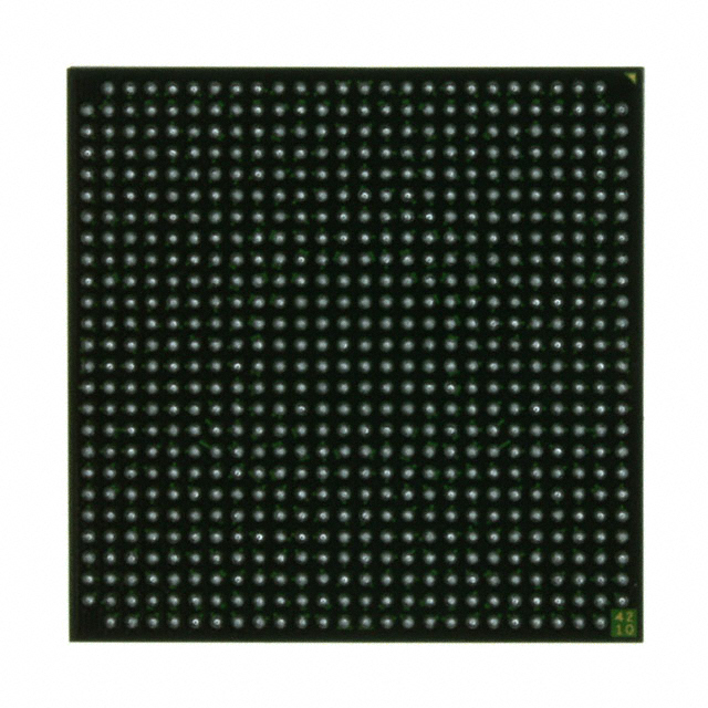
Virtex®-II Pro Field Programmable Gate Array (FPGA) IC 644 2506752 30816 1152-BBGA, FCBGA |
|---|---|
| Quantity | 1,481 Available (as of June 10, 2026) |

| Product Category | Field Programmable Gate Array (FPGA) |
|---|---|
| Manufacturer | AMD |
| Manufacturing Status | Obsolete |
| Manufacturer Standard Lead Time | Contact Us |
| Datasheet |
Specifications & Environmental
| Device Package | 1152-FCBGA (35x35) | Grade | Commercial | Operating Temperature | 0°C – 85°C | ||
|---|---|---|---|---|---|---|---|
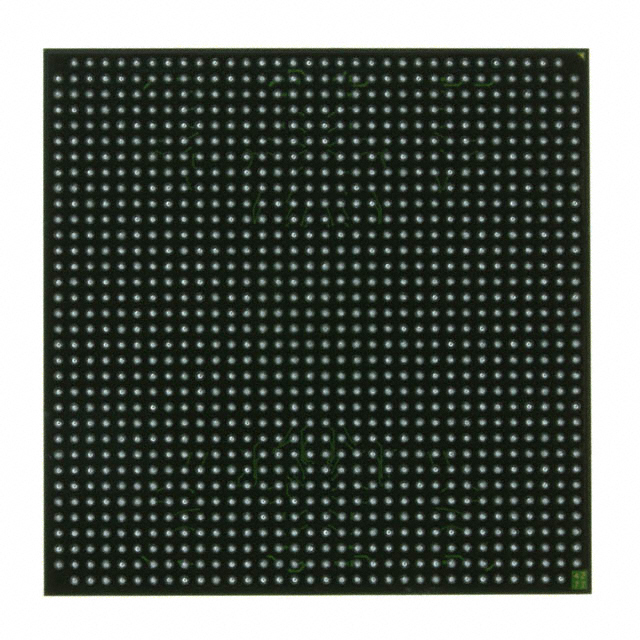
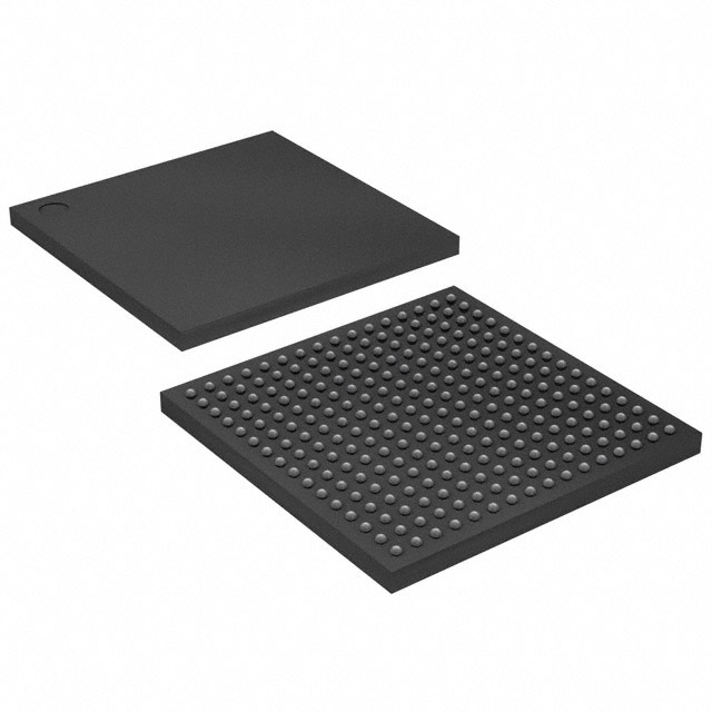
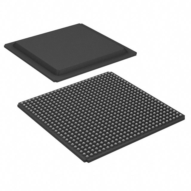
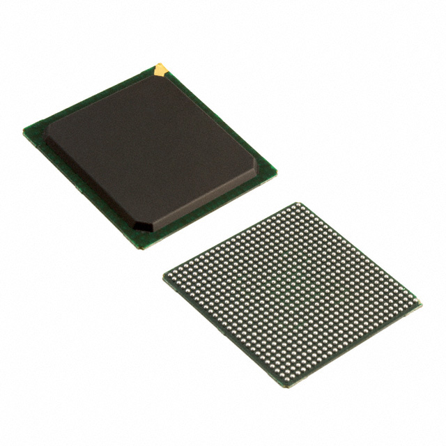
| Package / Case | 1152-BBGA, FCBGA | Number of I/O | 644 | Voltage | 1.425 V - 1.575 V | ||
| Mounting Method | Surface Mount | RoHS Compliance | ROHS3 Compliant | REACH Compliance | REACH Unaffected | ||
| Moisture Sensitivity Level | 4 (72 Hours) | Number of LABs/CLBs | 3424 | Number of Logic Elements/Cells | 30816 | ||
| Number of Gates | N/A | ECCN | 3A001A7A | HTS Code | 8542.39.0001 | ||
| Qualification | N/A | Total RAM Bits | 2506752 |
Overview of XC2VP30-7FFG1152C – Virtex®-II Pro FPGA, 1152-FCBGA
The XC2VP30-7FFG1152C is a Virtex®-II Pro Field Programmable Gate Array (FPGA) IC from AMD, offered in a 1152-ball FCBGA package for surface-mount assembly. It delivers high logic density and extensive I/O to address embedded processing, high-density interfacing, and system integration workloads.
Built on the Virtex-II Pro platform family architecture, this device targets designs that require large programmable logic resources, substantial on-chip memory, and a compact package footprint for commercial-temperature applications.
Key Features
- Logic Capacity 30,816 logic elements provide substantial programmable logic for complex digital functions and custom processing pipelines.
- Embedded Memory Approximately 2.5 Mbits of on-chip RAM (2,506,752 bits) for buffering, lookup tables, and data storage close to logic.
- High I/O Count 644 user I/O pins enable dense external interfacing and support for multiple parallel buses or mixed I/O domains.
- Compact Package 1152-FCBGA (35×35) package case in an FCBGA form factor, optimized for surface-mount PCB assembly and high pin-count routing.
- Supply Voltage Core supply range 1.425 V to 1.575 V for defined power rail planning in system designs.
- Commercial Temperature Grade Rated for 0 °C to 85 °C operation suitable for commercial electronics and controlled-environment equipment.
- Surface Mount Designed for surface-mount assembly methods commonly used in modern production lines.
- RoHS Compliant Manufactured to meet RoHS environmental requirements.
- Virtex-II Pro Family Features (series-level) The Virtex®-II Pro family includes platform capabilities such as embedded processor blocks and multi-gigabit transceiver support (family-level features described in the product series documentation).
Typical Applications
- Embedded Processing Platforms Use the programmable logic and on-chip memory to implement custom accelerators, control logic, and protocol handling in embedded systems.
- High‑Density I/O Systems Large 644-pin I/O count supports designs requiring multiple parallel interfaces, wide data buses, or mixed-signal front-ends.
- Telecom and Datacom Modules The Virtex-II Pro series architecture is suited to applications that need platform FPGA flexibility for high-bandwidth serial or parallel interfaces (see family documentation for transceiver and processor block details).
- System Integration and Prototyping High logic element count and embedded RAM make this device useful for consolidating multiple functions into a single FPGA during system-level prototyping and integration.
Unique Advantages
- High logic density: 30,816 logic elements enable implementation of complex state machines, datapaths, and custom compute blocks without external ASICs.
- Substantial on-chip RAM: Approximately 2.5 Mbits of embedded memory reduces reliance on external memory for buffering and LUT-based storage.
- Extensive external connectivity: 644 I/O pins simplify board-level routing for multi-channel systems and high-bandwidth interfaces.
- Space-efficient packaging: 1152-ball FCBGA (35×35) provides a dense pinout in a compact footprint for optimized PCB area usage.
- Predictable supply requirements: Defined core voltage range (1.425 V–1.575 V) facilitates power sequencing and regulator selection in system designs.
- RoHS-compliant and surface-mount ready: Meets environmental requirements and is compatible with standard SMT assembly processes.
Why Choose XC2VP30-7FFG1152C?
The XC2VP30-7FFG1152C positions itself as a flexible platform FPGA for commercial applications that demand a balance of high logic resources, on-chip memory, and a large number of I/O in a compact FCBGA package. Its specification set supports integration of complex digital functions and extensive interfacing while simplifying board-level design with a high pin-count BGA.
This device is well suited for engineering teams implementing embedded processing, high-density I/O subsystems, and system-level prototypes where predictable voltage and temperature requirements, along with RoHS compliance, are primary considerations.
Request a quote or submit an inquiry to receive availability and pricing for the XC2VP30-7FFG1152C. Our team will respond with full ordering information and assistance tailored to your project requirements.


Date Founded: 1969
Headquarters: Santa Clara, California, USA
Employees: 25,000+
Revenue: $22.68 Billion
Certifications and Memberships: ISO9001:2015, RoHS, REACH


