
XC2VP40-7FF1152C
| Part Description |
Virtex®-II Pro Field Programmable Gate Array (FPGA) IC 692 3538944 43632 1152-BBGA, FCBGA |
|---|---|
| Quantity | 1,076 Available (as of June 15, 2026) |
| Product Category | Field Programmable Gate Array (FPGA) |
|---|---|
| Manufacturer | AMD |
| Manufacturing Status | Obsolete |
| Manufacturer Standard Lead Time | Contact Us |
| Datasheet |
Specifications & Environmental
| Device Package | 1152-FCBGA (35x35) | Grade | Commercial | Operating Temperature | 0°C – 85°C | ||
|---|---|---|---|---|---|---|---|
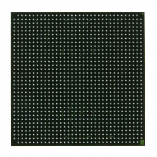
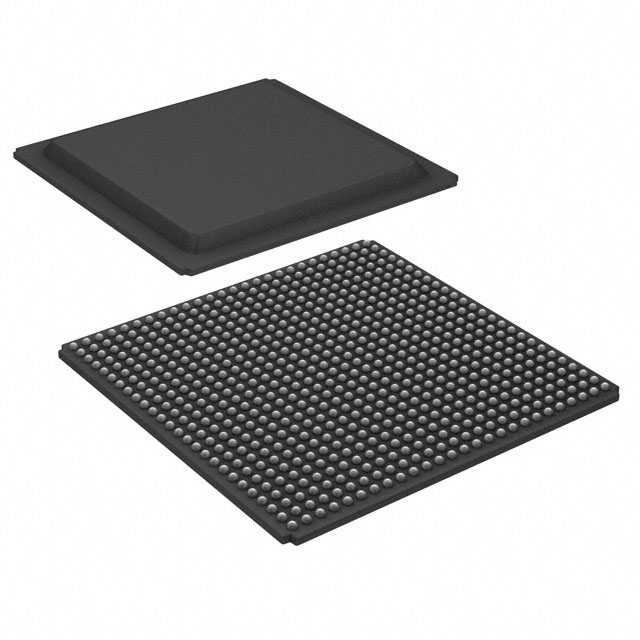
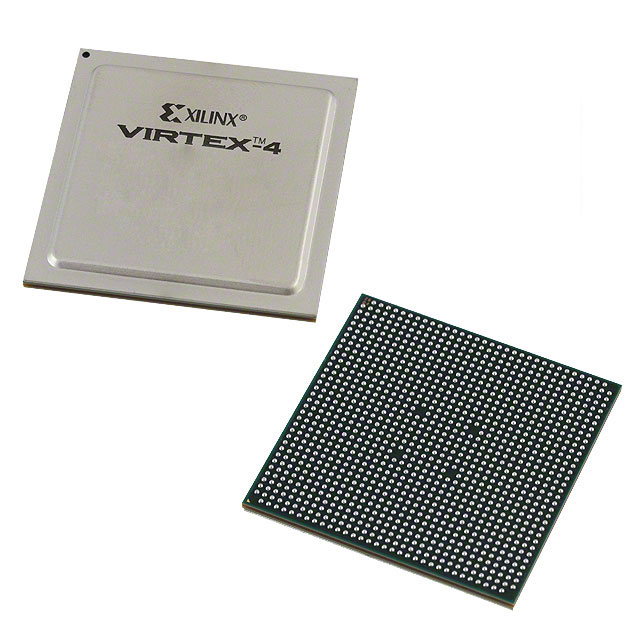
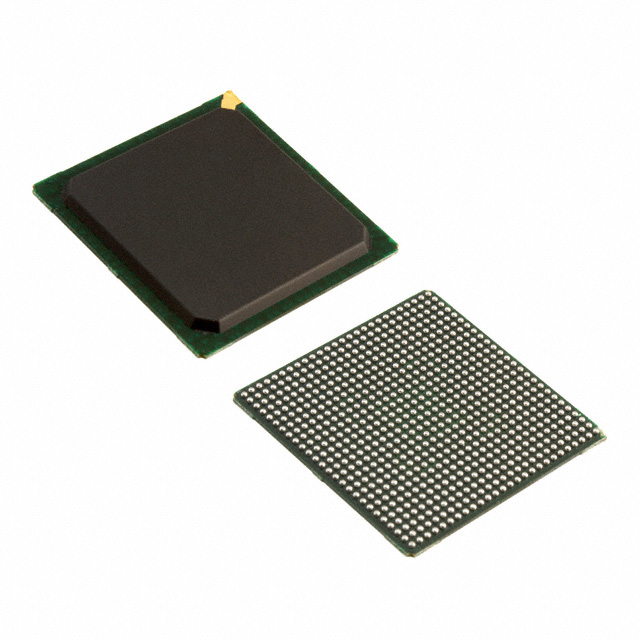
| Package / Case | 1152-BBGA, FCBGA | Number of I/O | 692 | Voltage | 1.425 V - 1.575 V | ||
| Mounting Method | Surface Mount | RoHS Compliance | RoHS non-compliant | REACH Compliance | REACH Unaffected | ||
| Moisture Sensitivity Level | 4 (72 Hours) | Number of LABs/CLBs | 4848 | Number of Logic Elements/Cells | 43632 | ||
| Number of Gates | N/A | ECCN | 3A991D | HTS Code | 8542.39.0001 | ||
| Qualification | N/A | Total RAM Bits | 3538944 |
Overview of XC2VP40-7FF1152C – Virtex-II Pro FPGA (1152-FCBGA)
The XC2VP40-7FF1152C is a Virtex®-II Pro field programmable gate array in a 1152-ball flip-chip BGA (35×35) package. It delivers high logic capacity, abundant I/O, and substantial on‑chip memory in a commercial‑grade FPGA targeted at complex embedded and system‑level applications.
This device is built for designs that require a combination of programmable logic, significant embedded memory, and high I/O density, supported by a nominal core supply range of 1.425 V to 1.575 V and an operating temperature range of 0 °C to 85 °C.
Key Features
- Logic Capacity 4,848 CLBs providing 43,632 logic elements to implement complex digital functions and control logic.
- Embedded Memory Approximately 3.54 Mbits of on‑chip RAM to support buffering, lookup tables, and state storage without external memory for many functions.
- High I/O Density 692 user I/Os to interface with multiple peripherals, parallel buses, and high‑pin‑count systems.
- Package 1152‑FCBGA (35×35) flip‑chip BGA package for compact board integration and high signal density.
- Power Core supply range specified at 1.425 V to 1.575 V to match standard FPGA power rails.
- Operating Range Commercial grade operation from 0 °C to 85 °C for standard embedded and industrial‑office environments.
- Mounting & Compliance Surface mount package; RoHS compliant for regulatory and manufacturing compatibility.
- Family Capabilities The Virtex‑II Pro family supports embedded processor integration and high‑speed serial interfaces — including up to two IBM PowerPC RISC processor blocks and RocketIO multi‑gigabit transceivers (family feature set documented in the datasheet).
Typical Applications
- Embedded System Controllers Use the device’s large logic capacity and embedded memory to implement system control, protocol handling, and custom hardware acceleration.
- Communications Equipment High I/O count and family support for multi‑gigabit transceivers make the FPGA suitable for network interface glue logic and data path processing.
- Data Acquisition & Processing On‑chip RAM and abundant logic elements enable real‑time data buffering, preprocessing, and signal conditioning tasks.
- Prototyping & Platform Development The device’s package and feature set support board‑level system prototypes and platform FPGA roles in development environments.
Unique Advantages
- Substantial Logic Resources: 43,632 logic elements combined with 4,848 CLBs provide headroom for complex designs and multiple concurrent functions.
- Significant Embedded Memory: Approximately 3.54 Mbits of on‑chip RAM reduces dependence on external memory for many buffering and stateful operations.
- Very High I/O Count: 692 I/Os offer flexibility for interfacing with dense connectors, parallel buses, and multi‑channel peripherals.
- Compact High‑Density Package: The 1152‑FCBGA (35×35) format enables dense board integration while supporting high pin counts.
- Commercial Temperature Rating: Rated for 0 °C to 85 °C operation to match a wide range of standard electronic applications.
- Standards‑Friendly Compliance: RoHS compliance simplifies regulatory and manufacturing processes for modern electronics production.
Why Choose XC2VP40-7FF1152C?
The XC2VP40-7FF1152C positions itself as a high‑capacity, high‑I/O Virtex‑II Pro FPGA tailored for system designers who need extensive programmable logic, embedded memory, and dense interfacing in a single package. Its combination of thousands of logic elements, multi‑megabit on‑chip RAM, and hundreds of I/Os supports complex control, data path, and prototyping tasks.
Designed for commercial applications, the device offers robust specifications for power and temperature and is RoHS compliant, making it suitable for a broad range of production and development projects that rely on scalable, programmable hardware building blocks.
If you would like pricing, availability, or a quote for XC2VP40-7FF1152C, please submit an inquiry or request a quote and our team will respond with the next steps.


Date Founded: 1969
Headquarters: Santa Clara, California, USA
Employees: 25,000+
Revenue: $22.68 Billion
Certifications and Memberships: ISO9001:2015, RoHS, REACH


